Method for forming a thin film light emitting device

a technology of light-emitting devices and thin films, which is applied in the direction of electroluminescent light sources, layered products, transportation and packaging, etc., can solve the problems of degrading the performance of metal cathodes, failure of devices, and difficult transit of electrons to organic light-emitting materials, so as to achieve effective raising the life of devices

Inactive Publication Date: 2006-01-10
DELTA OPTOELECTRONICS
View PDF7 Cites 1 Cited by
  • Summary
  • Abstract
  • Description
  • Claims
  • Application Information

AI Technical Summary

Benefits of technology

[0013]The invention provides a method for forming a thin film LED device. The method includes forming an active absorbing layer located on the cap layer of the LED device through vacuum evaporation manner. As the cap layer co

Problems solved by technology

If the energy band between the cathode material and the organic light emitting material is larger, electrons are more difficult to transit to the organic light emitting material.
The active material is very easy to react with water or oxygen, resulting in degrad

Method used


Image

  • Method for forming a thin film light emitting device
  • Method for forming a thin film light emitting device
  • Method for forming a thin film light emitting device

Examples


Embodiment Construction

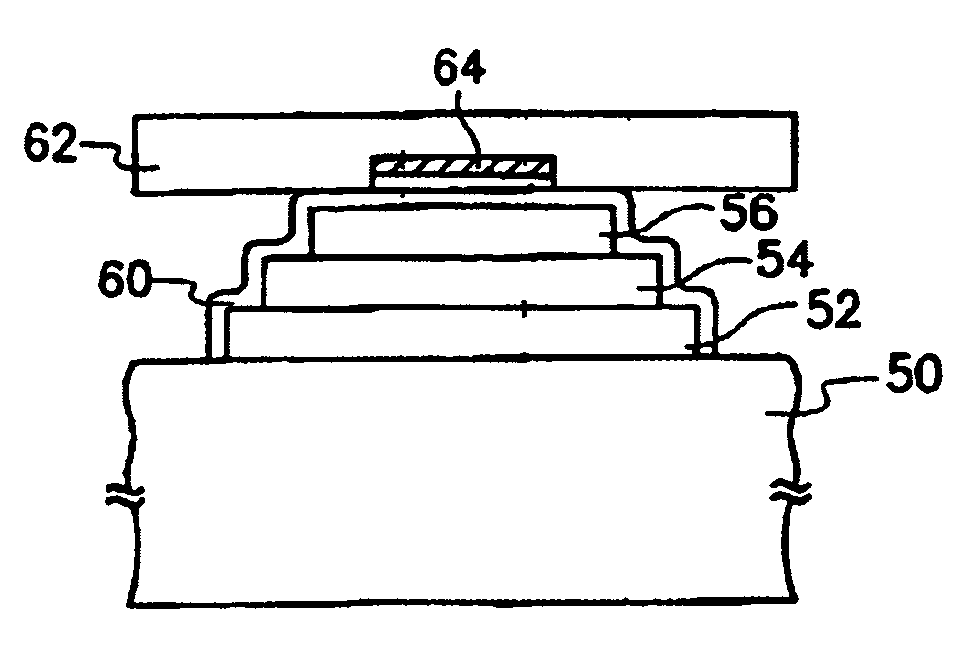
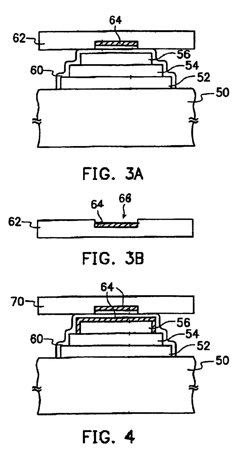
[0035]The invention particularly employs a vacuum evaporation process to deposit chemical active materials, such as active metal, onto a covering layer of a light emitting device to form an active absorption layer. As the covering layer covers over the metal cathode of the light emitting device, the active absorption layer can absorb invading water or oxygen, so as to avoid the erosion on the metal cathode and then prolong the lifetime of the product. In the invention, the evaporation process used to for the absorption layer has rendered several features, One is that the material suitable for use in evaporation is usually hydrophilic and can absorb water or oxygen. As a result, the active absorption layer formed by evaporation process naturally has the property to absorb water or oxygen.

[0036]Moreover, the invention has also employed an insulating layer, formed on the metal cathode before it is packaged. In this manner, even though the absorption is not included, the insulating laye...


PUM


Abstract

A method is to form a thin film light emitting device. The method includes providing a transparent substrate. A transparent anode layer, a light emitting layer, a metal cathode layer are sequentially formed on the transparent substrate. A sealant layer is formed to at least cover the light emitting layer and the metal cathode layer. A covering layer having a covering surface is provided. An evaporation process is performed to form an active absorption layer on the covering surface of the covering layer. The covering surface of the covering layer covers on a portion of the sealant layer above the metal cathode layer. The covering layer can have a recess region that is to be formed the active absorption layer thereon. Alternatively, the active absorption layer can be evaporated before the sealant is formed. Moreover, the active absorption layer can be replaced with an insulating layer.

Description

CROSS REFERENCE TO RELATED APPLICATION[0001]This application claims the priority benefit of Taiwan application serial no. 90106034, filed on Mar. 15, 2001.BACKGROUND OF THE INVENTION[0002]1. Field of the Invention[0003]The present invention relates to optoelectronics fabrication. Particularly, the present invention relates to a method for fabricating a thin film light emitting device, having a metal cathode with anti-oxidization function.[0004]2. Description of the Related Art[0005]The current optoelectronics technology has been successfully developed. The light emitting diode (LED) is one usual product of the optoelectronical devices. The light emitting diode can emit light when is applied with a bias. Thereby, the light emitting diode, associating with circuit design, can be incorporated in a display device, or providing as a light source. The light emitting diode has very wide applications.[0006]In general, LED can be characterized into two types. One type is metal semiconductor ...

Claims


Application Information

Patent Timeline
IPC IPC(8): H01L21/44H01L21/50H01L21/48H05B33/10H01L33/08H01L33/26H01L33/42H01L33/44H01L33/56H01L51/50H01L51/52H05B33/04
CPCH01L51/5237Y10T428/231H10K50/841H10K50/846H10K50/844
Inventor CHENG, CHEN LAIFEN, TSENG CHIUPAI, JUI-FENCHOU, YI-HUNGCHEN, YUNG-YUANWANG, PING-SONG
Owner DELTA OPTOELECTRONICS
Why Eureka
Try Eureka