Printed circuit board and electronic package using same

a printed circuit board and electronic package technology, applied in the direction of printed circuit aspects, printed circuit stress/warp reduction, electrical equipment construction details, etc., can solve the problems of lowering the reliability of the flip chip package, exfoliation of the insulating layer, etc., to reduce stress concentration, reduce stress, and reduce stress concentration

Inactive Publication Date: 2006-01-10
IBM CORP
View PDF10 Cites 70 Cited by
  • Summary
  • Abstract
  • Description
  • Claims
  • Application Information

AI Technical Summary

Benefits of technology

[0007]It is another object of this invention to provide a multi-layered printed circuit board adapted for having a semiconductor chip mounted thereon, that is part of an electronic package including a protection pad that substantially reduces stress concentration in an electrical connection between a circuit pattern on the printed circuit board and a conductive bump on a corner portion of the semiconductor chip.
[0008]According to one aspect of the invention, there is provided a printed circuit board adapted for having a semiconductor chip mounted thereon, the semiconductor chip including a conductive bump on a corner portion thereof, the circuit board comprising an insulating layer including a first surface, the first surface having first and second portions thereon, a circuit pattern positioned on the first portion of the first surface of the insulating layer and adapted for having an electrical connection thereon, for being electrically connected to the conductive bump on the corner portion of the semiconductor chip, and a protection pad positioned on the second portion of the first surface relative to the first portion so as to substantially reduce stress concentration in the electrical connection between the circuit pattern positioned on the first portion of the first surface of the insulating layer and the conductive bump of the semiconductor chip.
[0009]According to another aspect of the invention, there is provided a printed circuit board adapted for having a semiconductor chip mounted thereon, the semiconductor chip including a conductive bump on a corner portion thereof, the circuit board comprising an insulating layer including a first portion and a second portion positioned under the first portion, a circuit pattern positioned on

Problems solved by technology

Repeated temperature cycling can cause an open circuit or a near open circuit and the electrical connection to fail, thus lowering the reliability of the flip chip package.
Moreover, in a built-up multi-layered printed circuit board in which the circuit patterns are constituted in a number of layers, the stress

Method used


Image

  • Printed circuit board and electronic package using same
  • Printed circuit board and electronic package using same
  • Printed circuit board and electronic package using same

Examples


Embodiment Construction

[0019]For a better understanding of the present invention together with other and further objects, advantages and capabilities thereof, reference is made to the following disclosure and appended claims in connection with the above referenced drawings.

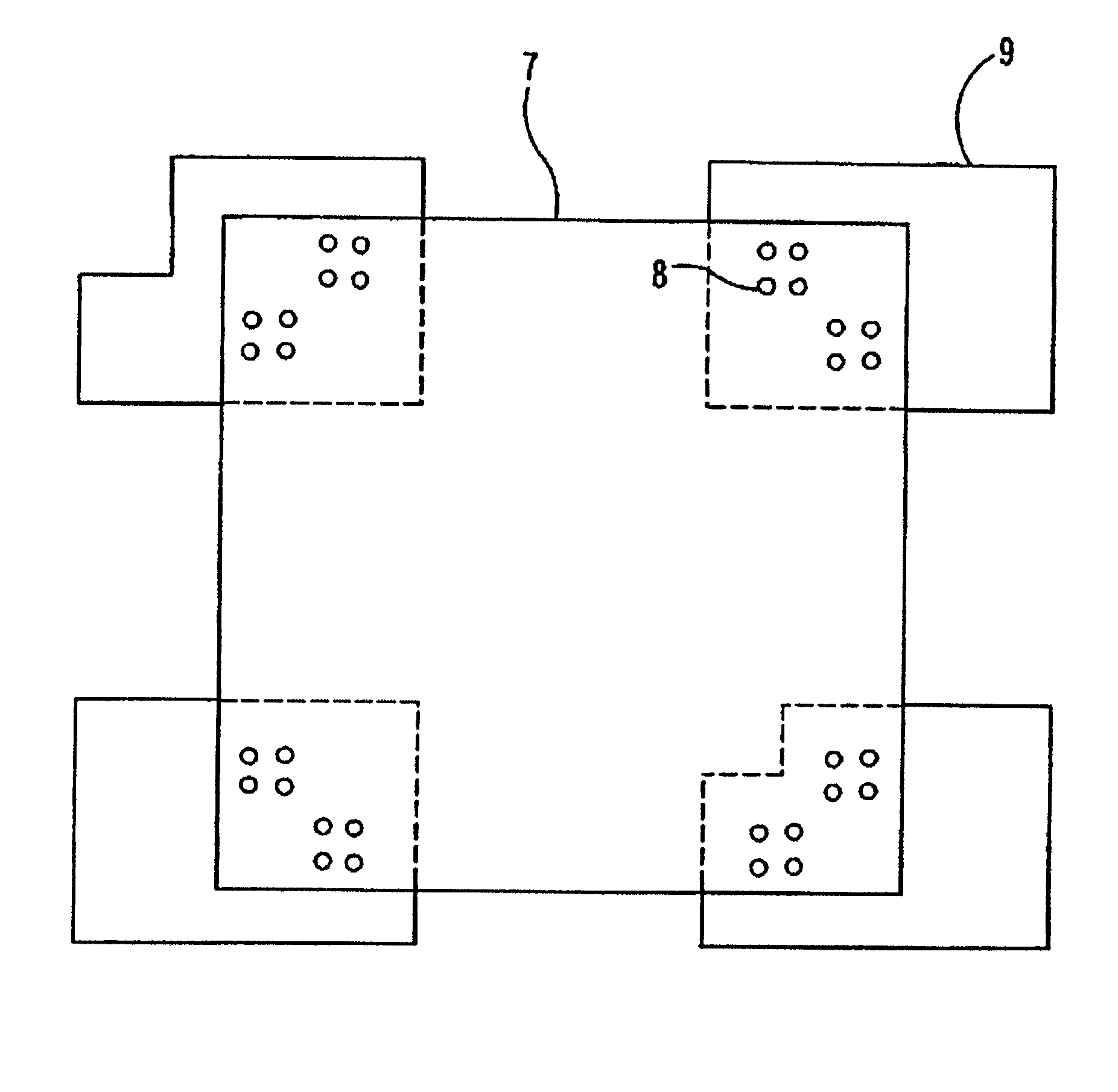
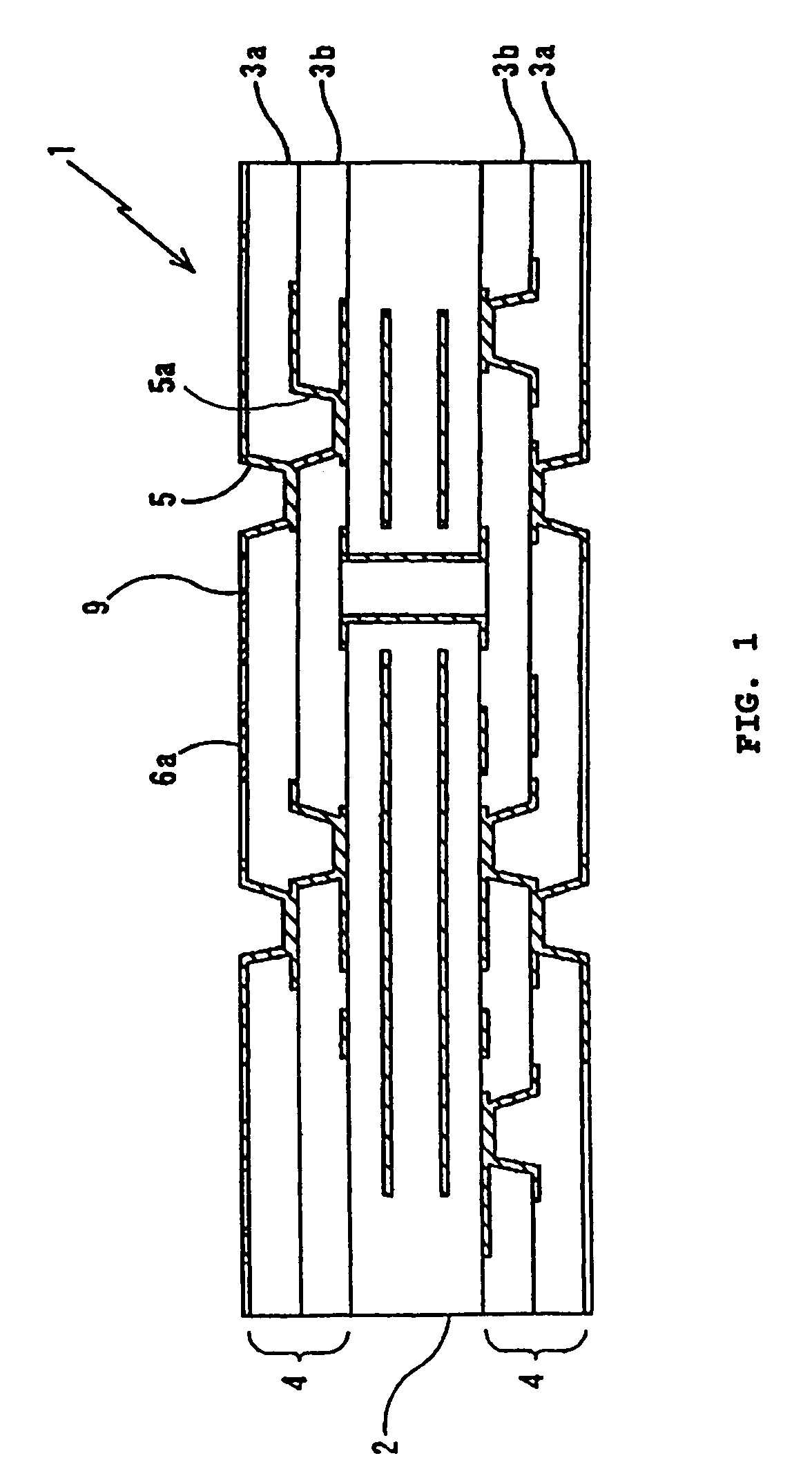
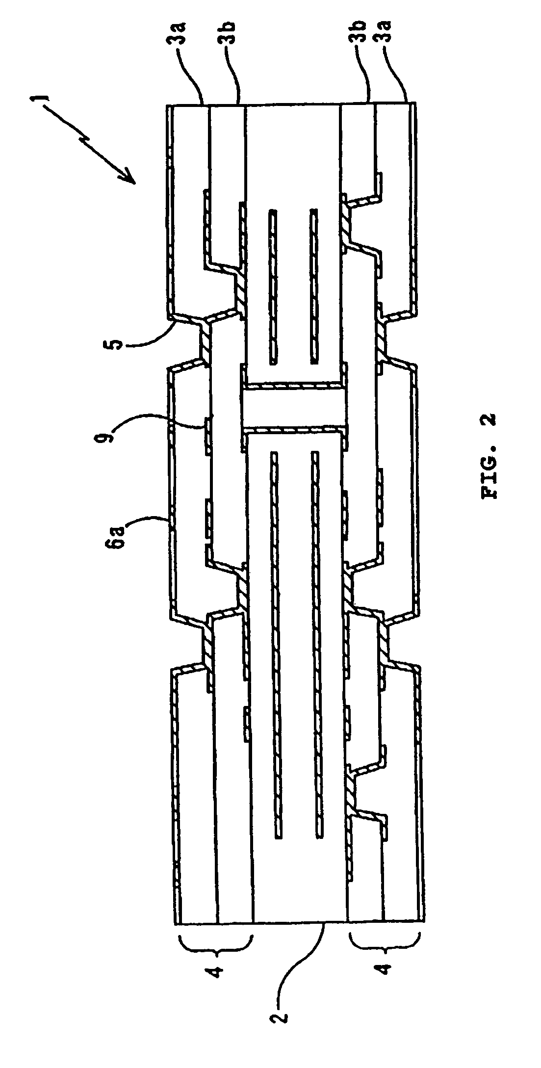
[0020]Referring to FIG. 1, an enlarged sectional view, in elevation, of one embodiment of the multi-layered printed circuit board 1 of the present invention is shown. The multi-layered printed circuit board 1, a built-up structure as shown, comprises a base substrate 2 and built-up portions 4, applied on both sides of the base substrate, each of the built-up portions being formed of insulating resin layers 3a and 3b. In one built-up portion 4, a via hole 5 and a circuit pattern 6a are formed. The base substrate 2 can be formed as a multi-layered plate with multiple layers, which comprises, for example, a glass epoxy substrate. In the present invention, base substrate 2 can be comprised of any known substrate.

[0021]The insulating resin l...


PUM


Abstract

A printed circuit board on which a semiconductor chip is flip chip mounted, comprising a circuit pattern to which a conductive bump, provided in a corner portion of a semiconductor chip, is connected, an insulating layer for holding the circuit pattern, and a protection pad which is positioned on the insulating layer relative to the circuit pattern, to which the conductive bump is connected.

Description

TECHNICAL FIELD[0001]The present invention relates to a printed circuit board for mounting a semiconductor chip, including a structure having a protection pad positioned on a portion of the printed circuit board to substantially reduce stress concentration in an electrical connection between a circuit pattern of the printed circuit board and a conductive bump on a corner portion of the semiconductor chip.BACKGROUND OF THE INVENTION[0002]Flip chip mounting is a mounting method in which a conductive bump is provided on each electrode pad portion of a semiconductor chip. These conductive bumps are electrically connected to circuit patterns on the surface of a printed circuit board to form a flip chip electronic package.[0003]These conductive bump and circuit patterns can be connected by means of a conductive paste-like adhesive containing fine silver particles. A conductive film interposer can be positioned between the conductive bumps and the circuit patterns. Heat and pressure can th...

Claims


Application Information

Patent Timeline
IPC IPC(8): H05K7/02H05K3/34H01L21/60H01L23/12H01L23/498H05K1/02H05K3/46
CPCH01L23/49822H01L23/49838H05K1/0271H01L2224/16H01L2924/01078H01L2924/01079H05K2201/2009H05K3/4602H05K3/4644H05K2201/09781H05K2201/10674H01L2924/00014H01L2224/0401
Inventor MORI, HIROYUKITSUKADA, YUTAKAYAMANAKA, KIMIHIRO
Owner IBM CORP
Why Eureka
Try Eureka