

Semiconductor memory having dummy regions in memory cell array
a memory cell array and memory cell technology, applied in the field of semiconductor memory having dummy regions in memory cell arrays, can solve the problems of destroying data held in memory cells, rewriting operations, and difficult layout design, so as to facilitate the formation of layered wiring, prevent memory cell array malfunction, and minimize the number of dummy regions
- Summary
- Abstract
- Description
- Claims
- Application Information
AI Technical Summary
Benefits of technology
Problems solved by technology
Method used
Image

Examples
Embodiment Construction
[0051]Embodiments of the present invention will be described below with reference to the drawings.
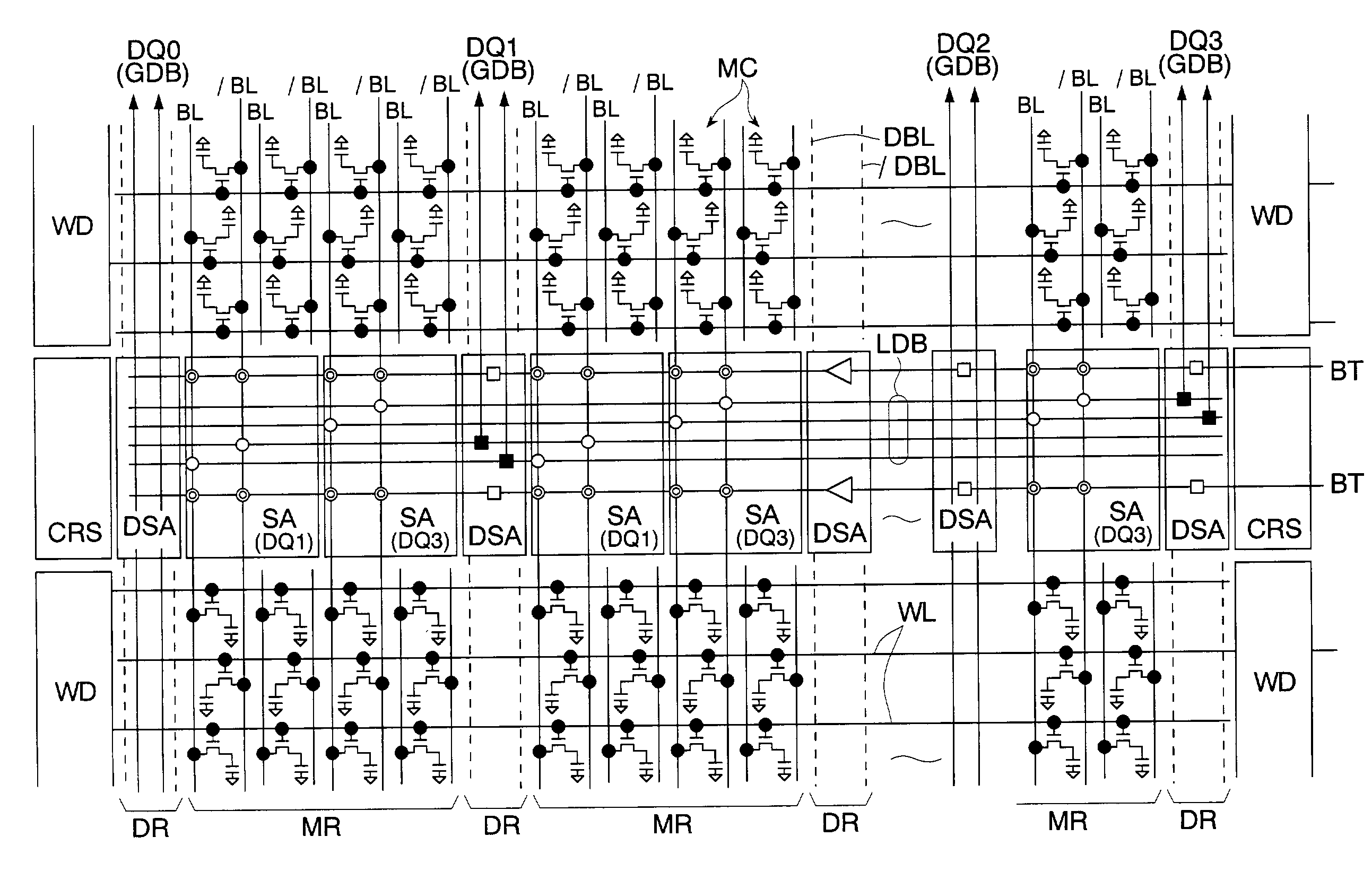
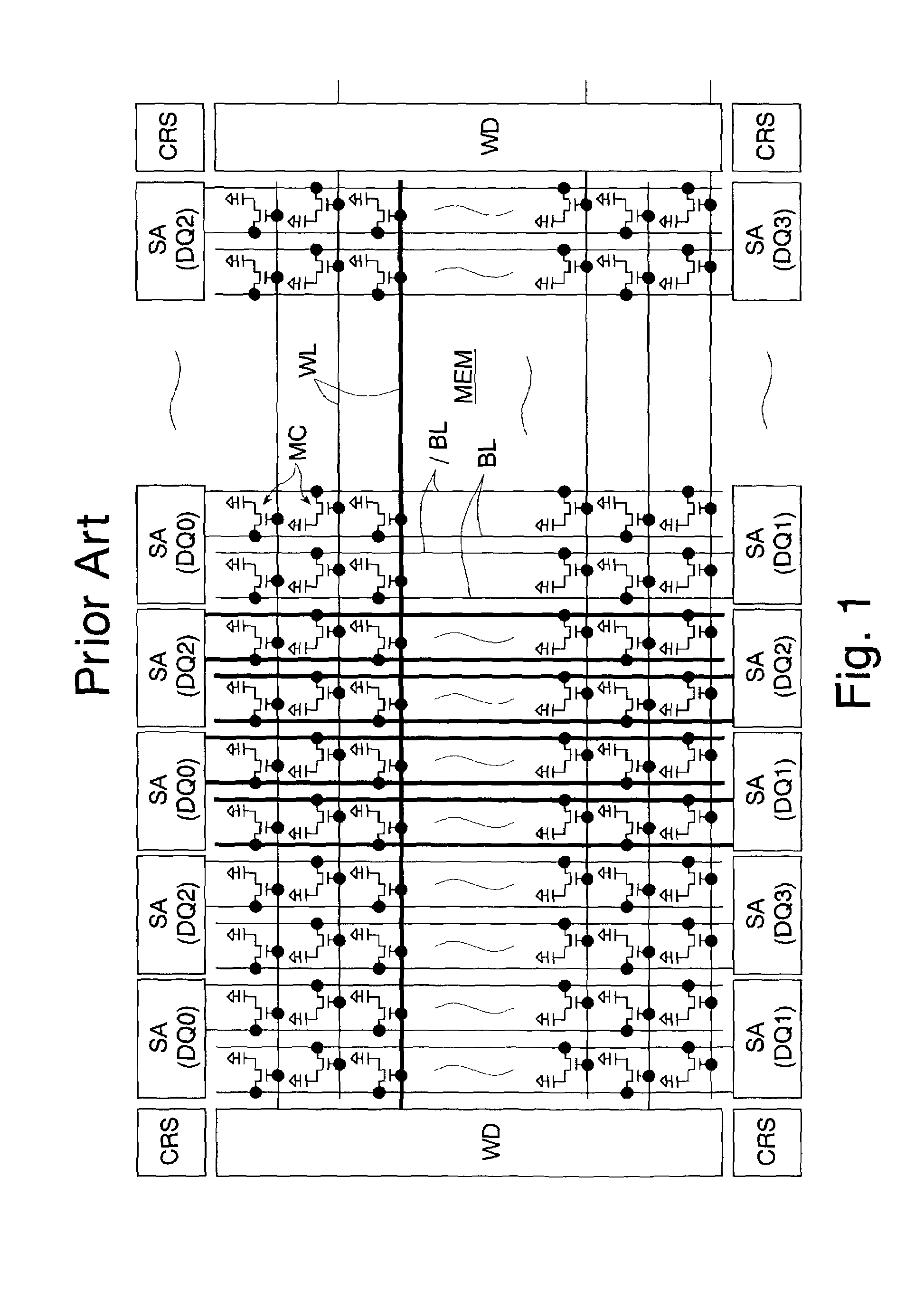
[0052]Referring to FIG. 3, there is shown a first embodiment of semiconductor memory according to the present invention. In this embodiment, elements corresponding to the same elements in the prior art of FIG. 1 are identified by the same reference designations and their detailed descriptions are omitted.
[0053]This semiconductor memory is formed, as a DRAM, on a silicon substrate by use of a CMOS process. The DRAM has a plurality of memory cell arrays ARY. Four-bit data are inputted to or outputted from each memory cell array ARY in one operation.
[0054]Each memory cell array ARY has a memory cell unit MEM; word decoders WD located on opposite sides (left and right of the figure) of the memory cell unit MEM; sense amplifiers SA located on the other opposite sides (upper and lower of the figure) thereof; and cross regions CRS located at the four corners thereof. The memory cell unit MEM i...
PUM
 Abstract
Description
Claims
Application Information