Liquid crystal panel and method of fabricating the same

a technology of liquid crystal panels and liquid crystal panels, applied in non-linear optics, instruments, optics, etc., to achieve the effect of high accuracy

Inactive Publication Date: 2006-01-24
BOE TECH GRP CO LTD
View PDF35 Cites 50 Cited by
  • Summary
  • Abstract
  • Description
  • Claims
  • Application Information

AI Technical Summary

Benefits of technology

[0016]In the method of fabricating the liquid crystal panel in accordance with the present invention, in the large substrate, the substrate forming-regions may be placed with a cutting projection line therebetween so that the sides provided with input-output terminals and terminals for conducting between substrates are directed in the opposite directions, and when the thin films for forming the alignment layers are formed, the thin films are formed in strip along the cutting projection line. If the thin films for forming the alignment layers are formed in strip, in flexographic p

Problems solved by technology

However, even if the accuracy of a flexographic printer is increased, it is not possible to control the printing region (the region marked by slanted broken lines in FIG. 12) of

Method used


Image

  • Liquid crystal panel and method of fabricating the same
  • Liquid crystal panel and method of fabricating the same
  • Liquid crystal panel and method of fabricating the same

Examples


first embodiment

(General Structure)

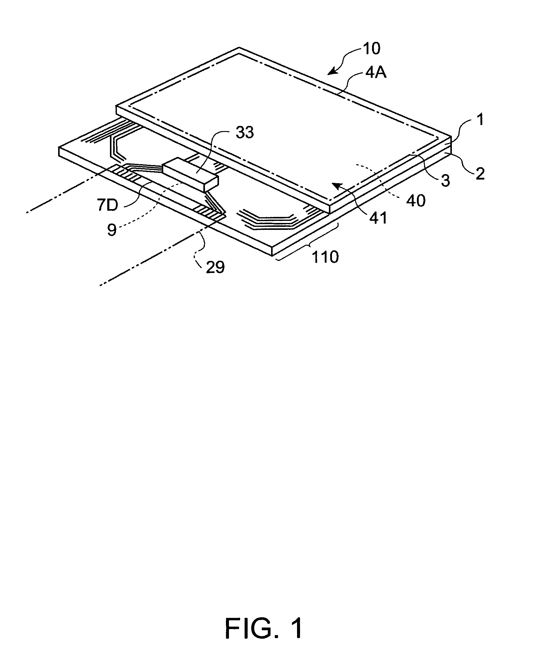
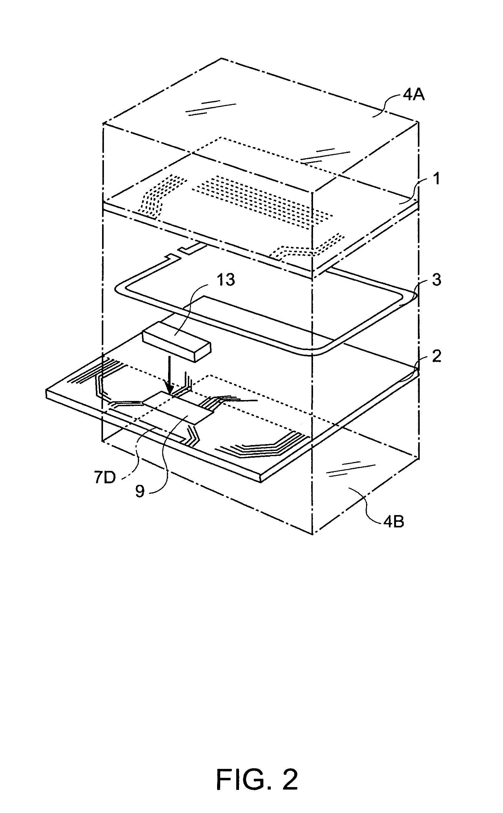
[0030]FIG. 1 is a perspective view of a liquid crystal display device and FIG. 2 is an exploded perspective view thereof. In FIGS. 1 and 2, only portions of wiring patterns and terminals are shown, and the details thereof are shown in FIGS. 3 and 4.

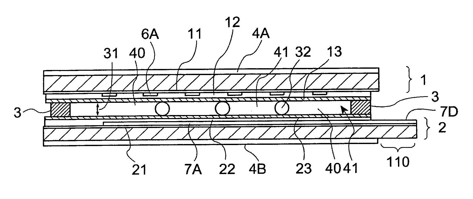
[0031]In FIGS. 1 and 2, a liquid crystal panel 10 of a liquid crystal display device mounted on an electronic apparatus such as a cordless telephone includes a first substrate 1 composed of transparent glass or the like and a second substrate 2 also composed of transparent glass or the like. A sealant 3 containing gap fillers and conductive particles is formed on one of the substrates by printing or the like, and the first substrate 1 and the second substrate 2 are bonded to each other with the sealant 3 therebetween. In this state, a predetermined gap is maintained between the first substrate 1 and the second substrate 2 by the gap fillers contained in the sealant 3, and a liquid crystal 40 is enclosed in the gap in a ...

second embodiment

[0057]FIG. 8 is a schematic diagram which shows first and second large substrates for forming a plurality of first and second substrates, respectively, regions for forming transparent insulation films and alignment layers (regions marked by broken lines slanting to the left) formed on the first and second large substrates, and regions for forming the sealant (regions marked by solid lines slanting to the right) in the fabrication process of a liquid crystal panel in accordance with a second embodiment of the present invention. Since the basic structure of the liquid crystal panel in this embodiment is in common with that of the liquid crystal panel in accordance with the first embodiment, the same numerals are used for the corresponding sections in FIG. 8, and the detailed description thereof will be omitted.

[0058]As shown in FIG. 8, in this embodiment, transparent insulation films 12 and 22 composed of silicon oxide films are formed on first and second large substrates 1A and 2A so...

third embodiment

[0060]FIG. 9 is a schematic diagram which shows first and second large substrates for forming a plurality of first and second substrates, respectively, regions for forming transparent insulation films and alignment layers (regions marked by broken lines slanting to the left) formed on the first and second large substrates, and regions for forming the sealant (regions marked by solid lines slanting to the right) in the fabrication process of a liquid crystal panel in accordance with a third embodiment of the present invention. Since the basic structure of the liquid crystal panel in this embodiment is in common with that of the liquid crystal panel in accordance with the first embodiment, the same numerals are used for the corresponding sections in FIG. 9, and the detailed description thereof will be omitted.

[0061]As shown in FIG. 9, in this embodiment, transparent insulation films 12 and 22 composed of silicon oxide films are formed on first and second large substrates 1A and 2A so ...


PUM


Abstract

In a liquid crystal panel 1 provided with first and second substrates 1 and 3 bonded by a sealant 3, alignment layers 13 and 23 for covering electrodes 6A and 7A, respectively, are formed up to the regions overlapping the regions for forming up to 3. Accordingly, since there is no space between the alignment 13 or 23 and the sealant 3, a low twist domain does not occur in a liquid crystal 40. Therefore, the vicinity of the inner periphery of the sealant can also be effectively used as the region for displaying images.

Description

TECHNICAL FIELD[0001]The present invention relates to liquid crystal panels used for liquid crystal display devices and methods of fabricating the same. More particularly, the invention relates to fabricating techniques for the individual substrates constituting the liquid crystal panels.BACKGROUND ART[0002]As shown in FIGS. 11(A) and 11(B), a first substrate 1 and a second substrate 2 constituting a liquid crystal panel 10 are bonded to each other by a sealant 3 with spacers 32 therebetween, leaving a predetermined gap. A liquid crystal 40 is enclosed in a gap 31. Polarizers 4A and 4B are attached to the first and second substrates 1 and 2, respectively. On the inner surface of the first substrate 1, electrodes 6A, which are composed of ITO (Indium Tin Oxide) films as transparent conductive films or the like for displaying various characters or for displaying dots, are formed on the surface of an underlayer protective film 11, which is composed of a silicon oxide film or the like; ...

Claims


Application Information

Patent Timeline
IPC IPC(8): G02F1/1337G02F1/1339
CPCG02F1/1337G02F1/1339G02F1/0107
Inventor NAKAHARA, HIROKIUEHARA, HIDEKIMIYAZAKI, TAKASHIHAGIWARA, TAKESHI
Owner BOE TECH GRP CO LTD
Why Eureka
Try Eureka