Method of making a bottom spin valve

a bottom spin valve and spin filter technology, applied in the field of gmr read head of the bottom spin valve structure, can solve the problems of adversely affecting the biasing, difficult to obtain a controllable bias point, and high gmr ratio (dr/r), and achieve the effect of enhancing the gmr ratio (dr/r) of the sensor, enhancing adhesion, and enhancing the anti-parallax configuration energetically favorabl

Inactive Publication Date: 2006-02-07
HEADWAY TECH INC
View PDF8 Cites 13 Cited by
  • Summary
  • Abstract
  • Description
  • Claims
  • Application Information

AI Technical Summary

Benefits of technology

[0017]Referring to FIG. 1 and the configuration above, it is first noted that the buffer (or seed) layer (10), the oxygen surfactant layer (52) formed on the spacer layer (24) and the oxidized capping layer (70) (oxidized during the pinned layer annealing process) are all used to greatly enhance the GMR ratio (dR / R) of the sensor. The buffer layer would typically be a layer of NiCr (with approximately 40% Cr by atomic weight) formed to a thickness of approximately 55 angstroms. The antiferromagnetic pinning layer (15) is normally a layer of antiferromagnetic material such as MnPt and is formed to a thickness of approximately 100 angstroms. The SyAF pinned layer (30) is a trilayer comprising a second ferromagnetic layer (32), a first ferromagnetic layer (36) and a coupling layer (34) of a material and critical thickness designed to coupled the magnetic moments of the ferromagnetic layers in antiparallel directions. Typical of the prior art would be second and first ferromagnetic layers both formed of CoFe and of approximate thicknesses 15 and 20 angstroms respectively. The coupling layer (34) producing the antiparallel magnetic moment configuration is typically a layer of Ru formed to a thickness of approximately 7.5 angstroms. This is a critical thickness as it is required to make the antiparallel configuration energetically favorable and variations in thickness not exceeding 0.5 angstroms are preferable. The magnetic moments of the two ferromagnetic layers are indicated as oppositely directed arrows (circle (41) and circle with cross (43)) normal to the cross-sectional plane of the drawing and the air bearing surface (ABS) of the sensor and are respectively out of and into the plane. This normal direction is hereinafter called the transverse direction. The surface of the non-magnetic spacer layer (50) separating the pinned layer from the free layer is treated in an oxygen ambient so that a very thin layer (sub-atomic mono-layer) of oxygen (52) is adsorbed on the surface distal from the pinned layer. This is the oxygen surfactant layer which generally enhances adhesion. As noted earlier, the spacer layer is a region of spin-dependent scattering of conduction electrons and its material composition and thickness is critical to obtaining the GMR effect of the sensor. Typically, the spacer layer is a layer of Cu formed to a thickness of approximately 18 angstroms. The ferromagnetic free layer (60) is formed on the oxygen surfactant layer of the spacer layer. This layer can be a single material layer or a composite layer and its thickness is critical to the definition of the resolution of the sensor. For example, for sensors operating in the 45 Gb / in2 range, a CoFe(10) / NiFe(20) composite free layer has been used, whereas for sensors operating in the 60 Gb / in2 range, a thinner composite CoFe(5) / NiFe(20) free layer has been used. The magnetization of the free layer is typically in the plane of the ABS and in the plane of the free layer itself, this direction being hereinafter referred to as the longitudinal direction, and is indicated in the figure as arrow (45). A high-conductance layer (HCL) (65) is then formed on the free layer, the HCL being typically a layer of Cu, which is a material with high conductivity, formed to a thickness of approximately 5 angstroms. The purpose of this layer is to direct the sensing current along the free layer and, thereby, to significantly reduce or eliminate the magnetic field of the sensing current as a mechanism for adversely affecting the free layer bias point. Finally, a capping layer is formed (70) on the HCL, typically a Ta layer approximately 10–20 angstroms thick. When this sensor stack is exposed to an oxidizing ambient during annealing to fix the magnetizations of the pinned and free layers, (or to an oxygen plasma used in reactive ion etching (RIE)), the capping layer (70) is oxidized to a depth depending upon the annealing time and temperature and a TaO insulating layer is formed which also serves as a specularly reflecting layer that greatly enhances sensor signal output. It is further noted that depending upon the type of conducting leads being formed, only selected regions of the capping layer may be oxidized. This will be further discussed in conjunction with the present invention as illustrated in FIG. 2b.

Problems solved by technology

Unfortunately, as the free layer is made increasingly thin, it becomes difficult to obtain a controllable bias point, a high GMR ratio (dR / R) and good softness (low coercivity).
Utilizing synthetic antiferromagnetic (SyAF) pinned layers (ferromagnetic layers coupled with their magnetic moments antiparallel) can reduce magnetostatic fields between the pinned and free layers which adversely affect the biasing; but if the free layer is sufficiently thin, even the magnetic fields produced by the sensing current have an adverse affect.
None of the art cited has specifically addressed the problem of free layer biasing for an ultra-thin free layer (less than 20 angstroms in thickness).

Method used


Image

  • Method of making a bottom spin valve
  • Method of making a bottom spin valve
  • Method of making a bottom spin valve

Examples


Embodiment Construction

[0023]To meet the objects of the present invention, the generic configuration of FIG. 1 will be replaced by either of the following preferred layer configurations i) and ii), each formed on an appropriate substrate (which is not indicated below):[0024]i) NiCr(55) / MP(100) / CoFe(13) / Ru(7.5) / CoFe(15) / Cu(18) / SL / CoFe(20) / Cu(5) / Ru(7.5–10) / Ta(10)[0025]ii) NiCr(55) / MP(100) / CoFe(13) / Ru(7.5) / CoFe(15) / Cu(18) / SL / CoFe(17) / Cu(3) / CoFe (3) / Ru(7.5–10) / Ta(10)

wherein the numbers in parentheses are preferred layer thicknesses in angstroms.

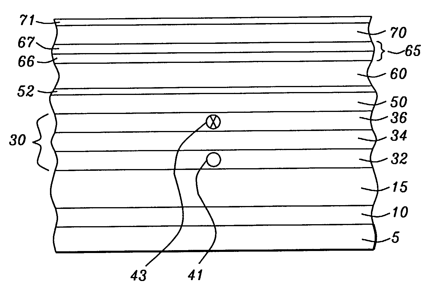
[0026]Referring first to FIG. 2a, there is seen in a schematic cross-sectional view the stack configuration described in i) above. Unlike the prior art of FIG. 1, this stack includes a single CoFe free layer (60) and a composite Cu / Ru high-conductance layer (65). Moving vertically upward in the figure, there is first seen a substrate (5) on which has been formed NiCr buffer layer (10), having approximately 40% Cr by atomic weight and formed to a thickness of between ap...


PUM

PropertyMeasurementUnit
thicknessaaaaaaaaaa
thicknessaaaaaaaaaa
thicknessaaaaaaaaaa

Abstract

Two embodiments of a GMR sensor of the bottom spin valve (BSV) spin filter spin valve (SFSV) type are provided, together with methods for their fabrication. In one embodiment, the sensor has an ultra thin (<20 angstroms) single free layer and a composite high-conductance layer (HCL), providing high output, low coercivity and positive magnetostriction. In a second embodiment, the sensor has a composite free layer and a single HCL, also having high output, low coercivity and positive magnetostriction. The sensors are capable of reading densities exceeding 60 Gb/in2.

Description

RELATED PATENT APPLICATION[0001]This application is related to Ser. No. 10 / 124,004 filing date Apr. 17, 2002, Ser. No. 10 / 308,597, filing date Dec. 3, 2002 all assigned to the same assignee as the current invention.BACKGROUND OF THE INVENTION[0002]1. Field of the Invention[0003]This invention relates generally to GMR read heads of the bottom spin valve structure and, more particularly, to a spin-filter type of bottom spin valve having an high-conductance layer and an ultra-thin CoFe free layer which has positive magnetostriction and high output.[0004]2. Description of the Related Art[0005]Magnetic read heads whose sensors make use of the giant magnetoresistive effect (GMR) in the bottom spin-valve configuration (BSV) are being increasingly required to read information recorded on magnetic media at ultra-high area densities (e.g. >45 Gb / in2). The typical BSV sensor configuration includes (in vertically ascending order) a pinning layer, a pinned layer, a conductive spacer layer, a ...

Claims


Application Information

Patent Timeline
Patent Type & Authority Patents(United States)
IPC IPC(8): G11B5/187G11B5/39G11B7/005
CPCG11B5/3906G11B7/0053Y10T29/49043Y10T29/49021Y10T29/49052Y10T29/49041Y10T29/49044Y10T29/49034Y10T29/49032
Inventor HORNG, CHENG T.TONG, RU-YING
Owner HEADWAY TECH INC
Why Eureka
Try Eureka