CoFe insertion for exchange bias and sensor improvement

a technology of exchange bias and cofe insertion, which is applied in the field of improved spin valves, can solve the problems of head stability problems, potential thermal reliability hazards, and limit the minimum thickness of seed layers and afm layers in current technology, and achieve the effects of reducing interlayer coupling, improving gmr ratio, and increasing hex between afm and pinned layers

Active Publication Date: 2006-03-23
HEADWAY TECH INC
View PDF15 Cites 32 Cited by
  • Summary
  • Abstract
  • Description
  • Claims
  • Application Information

AI Technical Summary

Benefits of technology

[0016] The first two objectives are achieved in a bottom spin valve structure in which a ferromagnetic insertion layer is introduced between a seed layer and an overlying AFM layer. The spin valve may be part of a GMR sensor, MTJ (magnetic tunnel junction), or TMR device, In the exemplary embodiment, a bottom spin valve is formed in a GMR sensor. A gap layer is disposed on a first shield that has been formed on a substrate. A NiCr seed layer which is the bottom layer in a spin valve stack is formed on the first gap layer. A key feature is that a ferromagnetic layer such as CoFe is inserted between the NiCr seed layer and an overlying AFM layer. In one embodiment, the spin valve stack is completed by sequentially forming a pinned layer, a copper spacer, a surfactant layer (SL), a free layer, and a cap layer above an IrMn AFM layer. The pinned layer preferably has a synthetic anti-parallel (SyAP) configuration in which a bottom AP2 layer comprised of CoFe is separated from an upper AP1 CoFe layer by a Ru coupling layer. Additionally, the AP2 layer may have a FeTa insertion layer to increase the exchange bias field as well as specular reflection therein. The free layer is comprised of a CoFe / FeNi bilayer and the cap layer preferably has a Ru / Ta configuration. The CoFe insertion layer is advantageously used to enable the NiCr seed layer thickness to be decreased from 45 Angstroms to 25 Angstroms without causing a thermal stability problem that is associated with thin seed layers in prior art. At the same time, the HEX between the AFM and pinned layer is increased and GMR ratio improves. The CoFe insertion layer also allows the AFM layer thickness to be reduced somewhat and thereby decreases the interlayer coupling with the free layer, increases the GMR ratio further, and improves free layer properties.
[0017] One method of forming the desired GMR sensor involves deposition of all the spin valve layers in a magnetron sputtering process. A key step is the deposition of the NiCr seed layer on the first gap layer. The inventors have discovered that a low Ar flow rate of about 10 standard cubic centimeters per minute (sccm) improves the growth morphology of the NiCr layer such that this seed layer can be thinned somewhat without lowering HEX and Tb. Another important step is implementing a high Ar flow rate during the AFM deposition of about 100 sccm. The remaining spin valve layers are deposited with a standard Ar flow rate of about 40 sccm. In one embodiment, the GMR sensor is fabricated by patterning a photoresist layer on the spin valve stack, ion beam etching to remove unwanted portions of the stack, and depositing a seed layer, hard bias layer, and leads adjacent to the sidewalls of the resulting GMR element. The photoresist layer is lifted off and then a second gap layer and a second shield are disposed on the leads and GMR element to complete the sensor.

Problems solved by technology

However, there is a limit to the minimum thickness for seed layers and AFM layers in current technology.
Due to the finite size effect, thinning the AFM layer thickness will eventually cause the blocking temperature to drop significantly and thereby produce a potential hazard in thermal reliability.
If the seed layer is too thin, the AFM grains that contribute to the exchange bias cannot be established which results in a head stability problem.
Besides failing to achieve a large enough exchange bias field (HEX), improper AFM grain size will lead to a large magnetic training effect.

Method used


Image

  • CoFe insertion for exchange bias and sensor improvement
  • CoFe insertion for exchange bias and sensor improvement
  • CoFe insertion for exchange bias and sensor improvement

Examples


Embodiment Construction

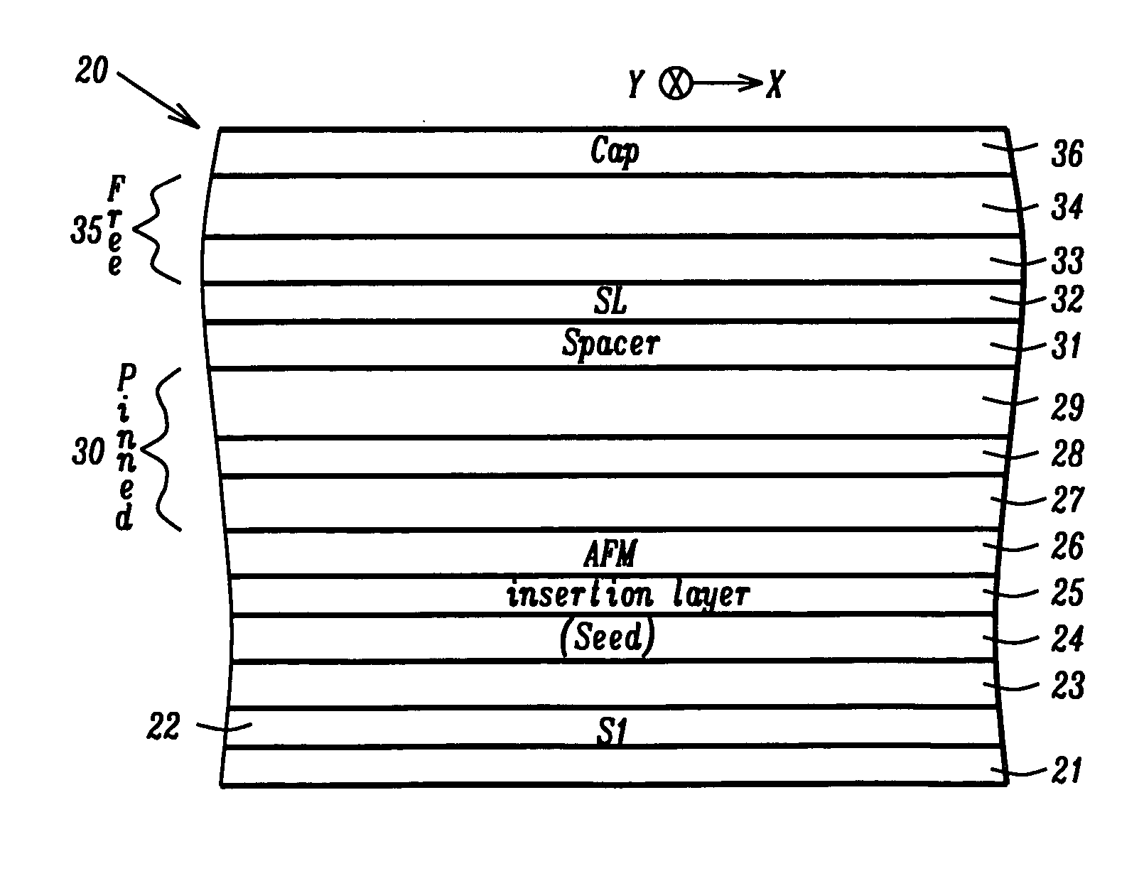
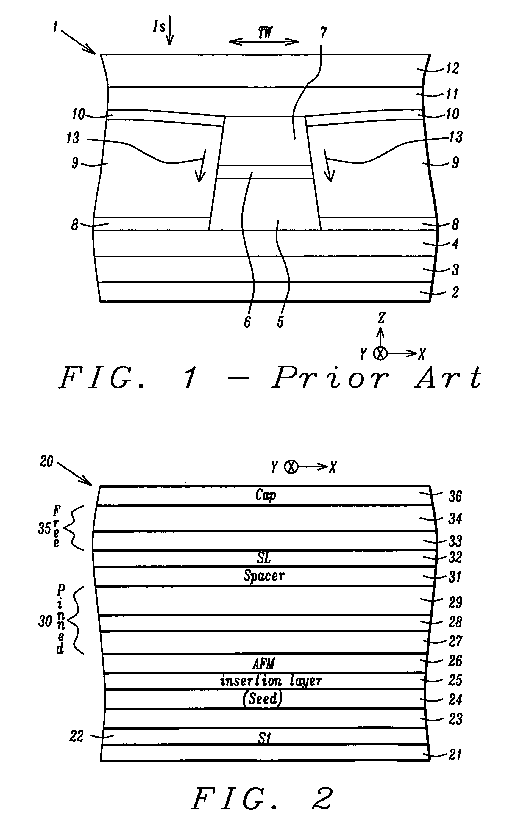
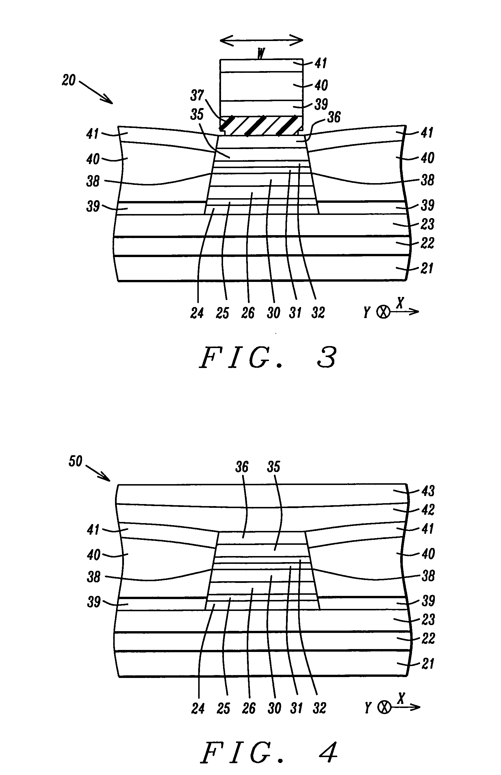
[0022] The present invention is a spin valve structure that may be used in a sensor of a read head in a magnetic recording device and a method for making the same. The spin valve structure is especially suited for an ultra-high magnetic recording device wherein the recording density is greater than about 100 Gbits / in2. The drawings are provided by way of example and are not intended to limit the scope of the invention. Although a bottom spin valve structure is described in the exemplary embodiment, those skilled in the art will appreciate that the seed layer / insertion layer / AFM configuration described herein may be incorporated in other applications including but not limited to a dual spin valve, CPP spin valve, MTJ, and TMR (tunneling magnetoresistive) devices. In other words, a ferromagnetic insertion layer may be added between a seed layer and adjacent AFM layer according to the present invention in any device based on a magnetoresistive effect.

[0023] A novel spin valve structur...


PUM

PropertyMeasurementUnit
thicknessaaaaaaaaaa
thicknessaaaaaaaaaa
thicknessaaaaaaaaaa

Abstract

A GMR spin value structure with improved performance and a method for making the same is disclosed. A key feature is the incorporation of a thin ferromagnetic insertion layer such as a 5 Angstrom thick CoFe layer between a NiCr seed layer and an IrMn AFM layer. Lowering the Ar flow rate to 10 sccm for the NiCr sputter deposition and raising the Ar flow rate to 100 sccm for the IrMn deposition enables the seed layer to be thinned to 25 Angstroms and the AFM layer to about 40 Angstroms. As a result, HEX between the AFM and pinned layers increases by up to 200 Oe while the Tb is maintained at or above 250° C. When the seed/CoFe/AFM configuration is used in a read head sensor, a higher GMR ratio is observed in addition to smaller free layer coercivity (HCF), interlayer coupling (HE), and HK values.

Description

FIELD OF THE INVENTION [0001] The invention relates to an improved spin valve for use in a giant magnetoresistive (GMR) sensor in a magnetic read head and to a method for making the same. In particular, a ferromagnetic insertion layer is used between a seed layer and AFM layer to enhance the exchange bias field, increase blocking temperature, and improve the magnetoresistive effect as well as the free layer softness. BACKGROUND OF THE INVENTION [0002] A magnetic disk drive includes read and write heads that may form a merged head attached to a slider on a positioning arm. During a read or write operation, the read and write heads are suspended over a magnetic disk on an air bearing surface (ABS). The read head has a sensor which is a critical component since it is used to detect magnetic field signals by a resistance change. One form of magnetoresistance is a spin valve magnetoresistance (SVMR) or giant magnetoresistance (GMR) which is based on a configuration in which two ferromagn...

Claims


Application Information

Patent Timeline
Patent Type & Authority Applications(United States)
IPC IPC(8): G11B5/33G11B5/127
CPCB82Y10/00B82Y25/00G11B2005/3996G11B5/3929G01R33/093
Inventor ZHANG, KUNLIANGWANG, HUI-CHUANZHAO, TONGLI, MINTORNG, CHYU-JIUH
Owner HEADWAY TECH INC
Why Eureka
Try Eureka