High efficiency crossed slot microstrip antenna

a microstrip antenna and high efficiency technology, applied in the direction of slot antennas, antenna details, antennas, etc., can solve the problems of inability to meet the requirements of inability to meet the requirements of a given substrate, and the line width required for exceptionally high or low characteristic impedance values can be too narrow or too wide for practical implementation on a given substrate, etc., to achieve different substrate properties.

Inactive Publication Date: 2006-02-07
HARRIS CORP
View PDF45 Cites 39 Cited by
  • Summary
  • Abstract
  • Description
  • Claims
  • Application Information

AI Technical Summary

Problems solved by technology

If the impedance of different parts of the circuit do not match, signal reflections and inefficient power transfer can result.
As noted, one problem encountered when designing microelectronic RF circuitry is the selection of a dielectric board substrate material that is reasonably suitable for all of the various passive components, radiating elements and transmission line circuits to be formed on the board.
Similarly, the line widths required for exceptionally high or low characteristic impedance values can, in many instances, be too narrow or too wide for practical implementation for a given substrate.
Still, an optimal board substrate material design choice for some components may be inconsistent with the optimal board substrate material for other components, such as antenna elements.
Moreover, some design objectives for a circuit component may be inconsistent with one another.
However, the use of a dielectric with a high relative permittivity will generally result in a significant reduction in the radiation efficiency of the antenna.
Dielectric loss is generally due to the imperfect behavior of bound charges, and exists whenever a dielectric material is placed in a time varying electrical field.
Dielectric loss generally increases with operating frequency.
However, the use of a dielectric material having a low dielectric constant can present certain disadvantages, such as the inability to efficiently focus radiated power from the feed line through the slot for slot fed antennas.
Unfortunately, the performance of crossed slot microstrip antennas is compromised through selection of a particular dielectric material which has a single uniform dielectric constant.
However, a low dielectric constant dielectric material in the junction region between the slot and the feed generally results in poor antenna radiation efficiency due to poor coupling characteristics through the slot.
As a result, a conventional dielectric material selected must necessarily compromise either the loss characteristics or the efficiency of the antenna.

Method used


Image

  • High efficiency crossed slot microstrip antenna
  • High efficiency crossed slot microstrip antenna
  • High efficiency crossed slot microstrip antenna

Examples


Embodiment Construction

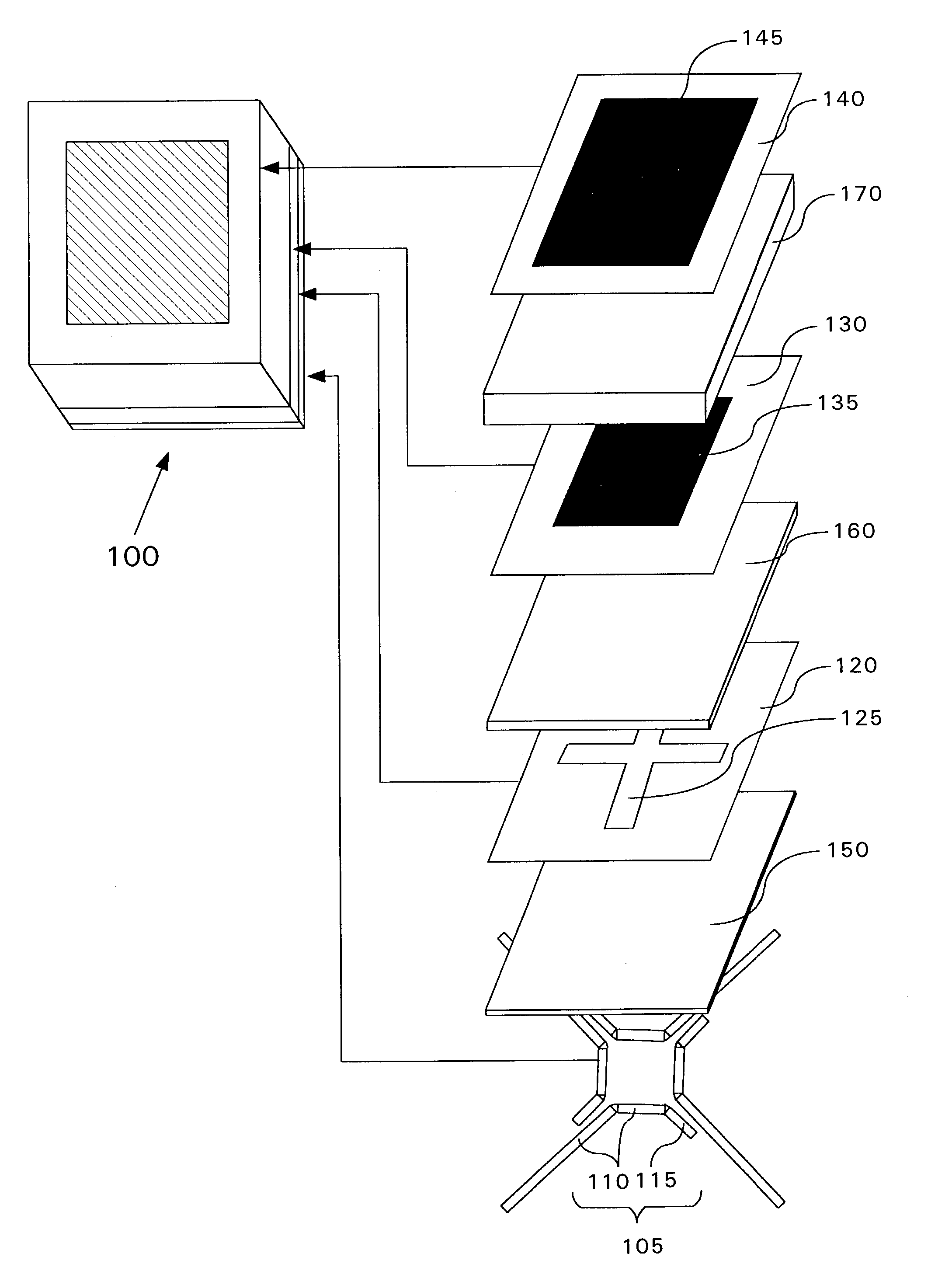
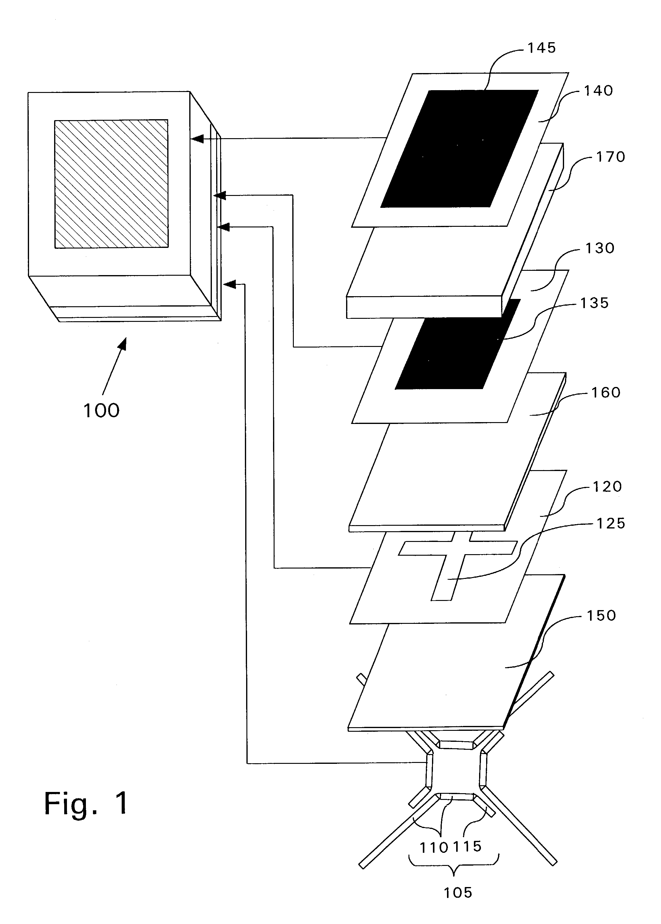
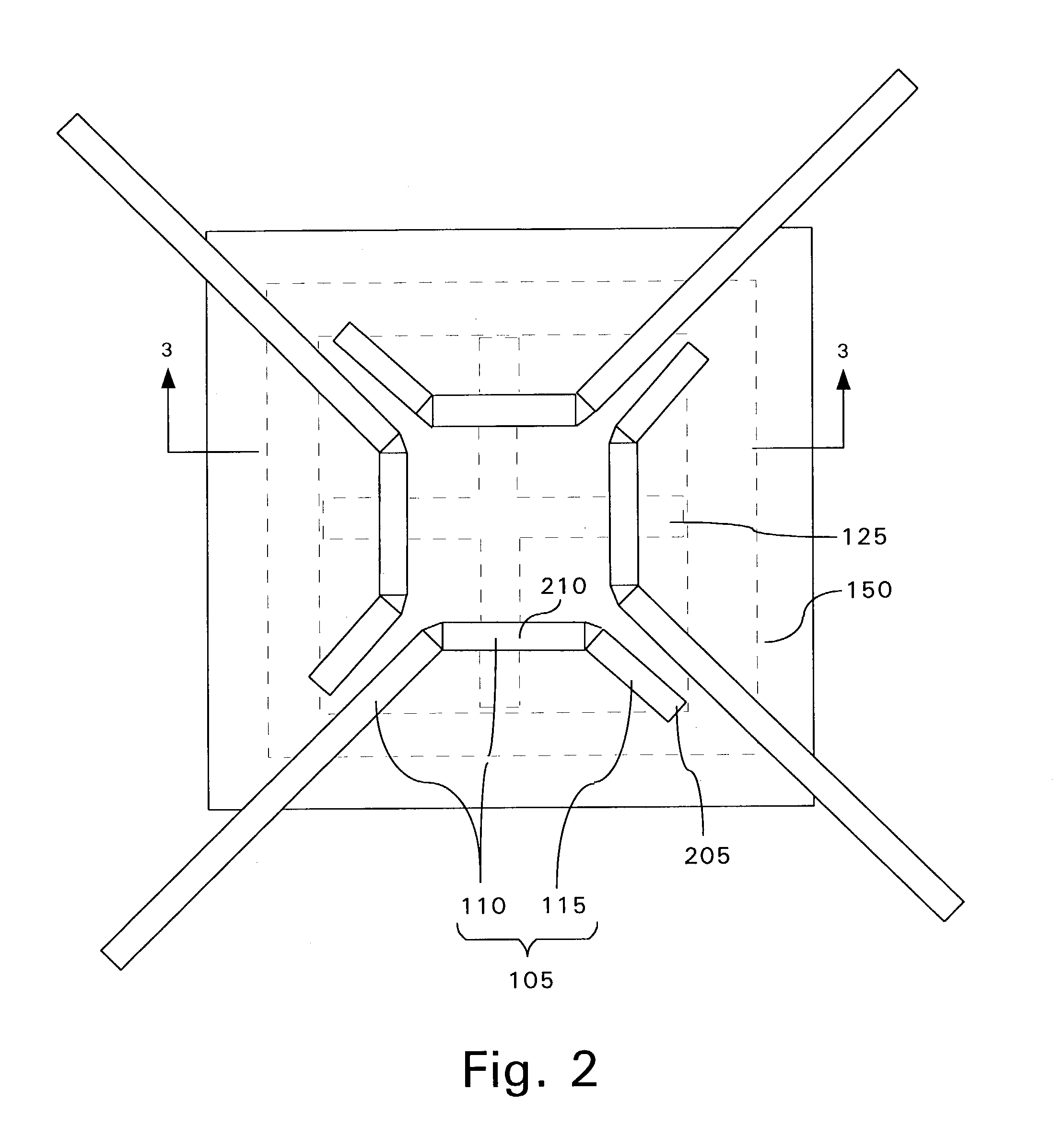
[0027]A crossed slot fed microstrip antenna has reduced size, but provides increased efficiency. The crossed slot fed microstrip antenna may also provide enhanced bandwidth. The improved microstrip antenna is formed by locally controlling the effective permittivity and / or effective permeability of one or more dielectric layer portions comprising the antenna.

[0028]Low dielectric constant board materials are ordinarily selected for RF designs. For example, polytetrafluoroethylene (PTFE) based composites such as RT / duroid® 6002 (dielectric constant of 2.94; loss tangent of 0.009) and RT / duroid® 5880 (dielectric constant of 2.2; loss tangent of 0.0007) are both available from Rogers Microwave Products, Advanced Circuit Materials Division, 100 S. Roosevelt Ave, Chandler, Ariz. 85226. Both of these materials are common board material choices. The above board materials are uniform across the board area in terms of thickness and physical properties and provide dielectric layers having relat...


PUM


Abstract

A crossed slot fed microstrip antenna (100). The antenna (100) includes a conducting ground plane (125), which has at least one crossed slot (125), and at least two feed lines (105). The feed lines (105) have respective stub regions (115) that extend beyond the crossed slot (125) and transfer signal energy to or from the crossed slot (125). The antenna (100) also includes a first substrate (150) disposed between the ground plane (120) and the feed lines (105). The first substrate (150) includes a first region and at least a second region, the regions having different substrate properties. The first region is proximate to at least one of the feed lines (105).

Description

BACKGROUND OF THE INVENTION[0001]1. Statement of the Technical Field[0002]The inventive arrangements relate generally to microstrip antennas and more particularly to crossed slot fed microstrip antennas.[0003]2. Description of the Related Art[0004]RF circuits, transmission lines and antenna elements are commonly manufactured on specially designed substrate boards. Conventional circuit board substrates are generally formed by processes such as casting or spray coating which typically result in uniform substrate physical properties, including the dielectric constant.[0005]For the purposes RF circuits, it is generally important to maintain careful control over impedance characteristics. If the impedance of different parts of the circuit do not match, signal reflections and inefficient power transfer can result. Electrical length of transmission lines and radiators in these circuits can also be a critical design factor.[0006]Two critical factors affecting circuit performance relate to t...

Claims


Application Information

Patent Timeline
Patent Type & Authority Patents(United States)
IPC IPC(8): H01Q1/38H01Q9/04
CPCH01Q1/38H01Q9/0442H01Q9/0435H01Q9/0414H01Q9/0485H01Q13/106
Inventor KILLEN, WILLIAM D.PIKE, RANDY T.DELGADO, HERIBERTO JOSE
Owner HARRIS CORP
Why Eureka
Try Eureka