Method for reducing dark current

a technology of dark current and charge, applied in the field of charge coupled devices, can solve the problems of thermally generated charge, low conductance of channel stops, undesirable dark current, etc., and achieve the effect of reducing dark current and avoiding p-well boun

Inactive Publication Date: 2006-02-07
SEMICON COMPONENTS IND LLC
View PDF19 Cites 30 Cited by
  • Summary
  • Abstract
  • Description
  • Claims
  • Application Information

AI Technical Summary

Benefits of technology

[0014]It is an object of this invention to reduce the dark current which is generated during the horizontal read-out, period.
[0015]It is a further object of the present invention to eliminate the need for added conductors in CCD image sensing devices operating in the, so called, accumulation mode of clocking.
[0016]It is still

Problems solved by technology

The conductance of these channel stops, however, is relatively low and, in certain circumstances, additional means are required to provide needed conductivity for the movement of the holes.
Dark current is undesirable because the thermally generated charge cannot be easily distinguished from the signal charges produced by light exposure.
It is during this period of quiescence that dark current problems arise in the vertical shift registers.
All three sources, result in spurious charges being collected as signal in the buried channel.
For large devices, the net charge that must be moved in this way is significantly impeded by the relatively high resistance of the p-type regions.
While this is true for any CCD ope

Method used


Image

  • Method for reducing dark current
  • Method for reducing dark current
  • Method for reducing dark current

Examples


Embodiment Construction

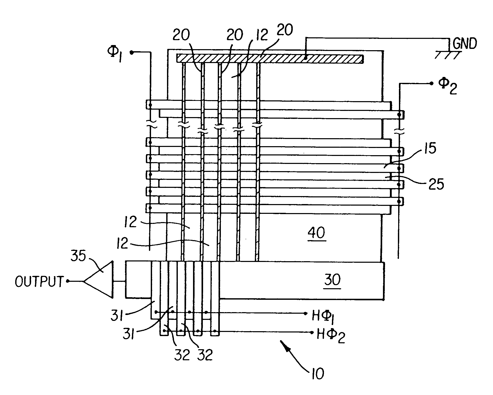
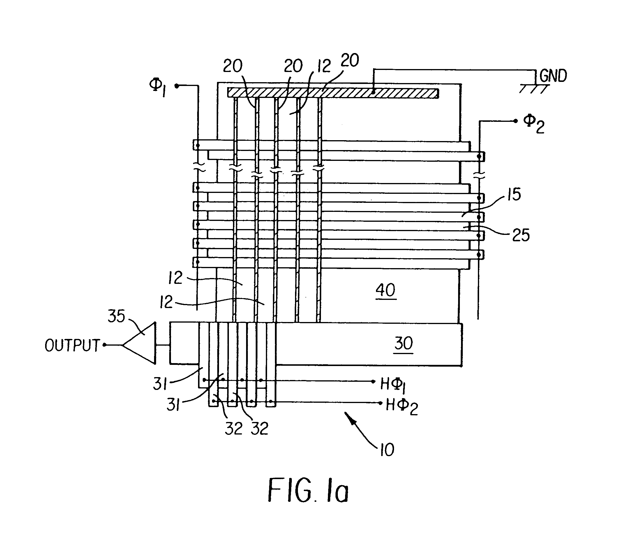
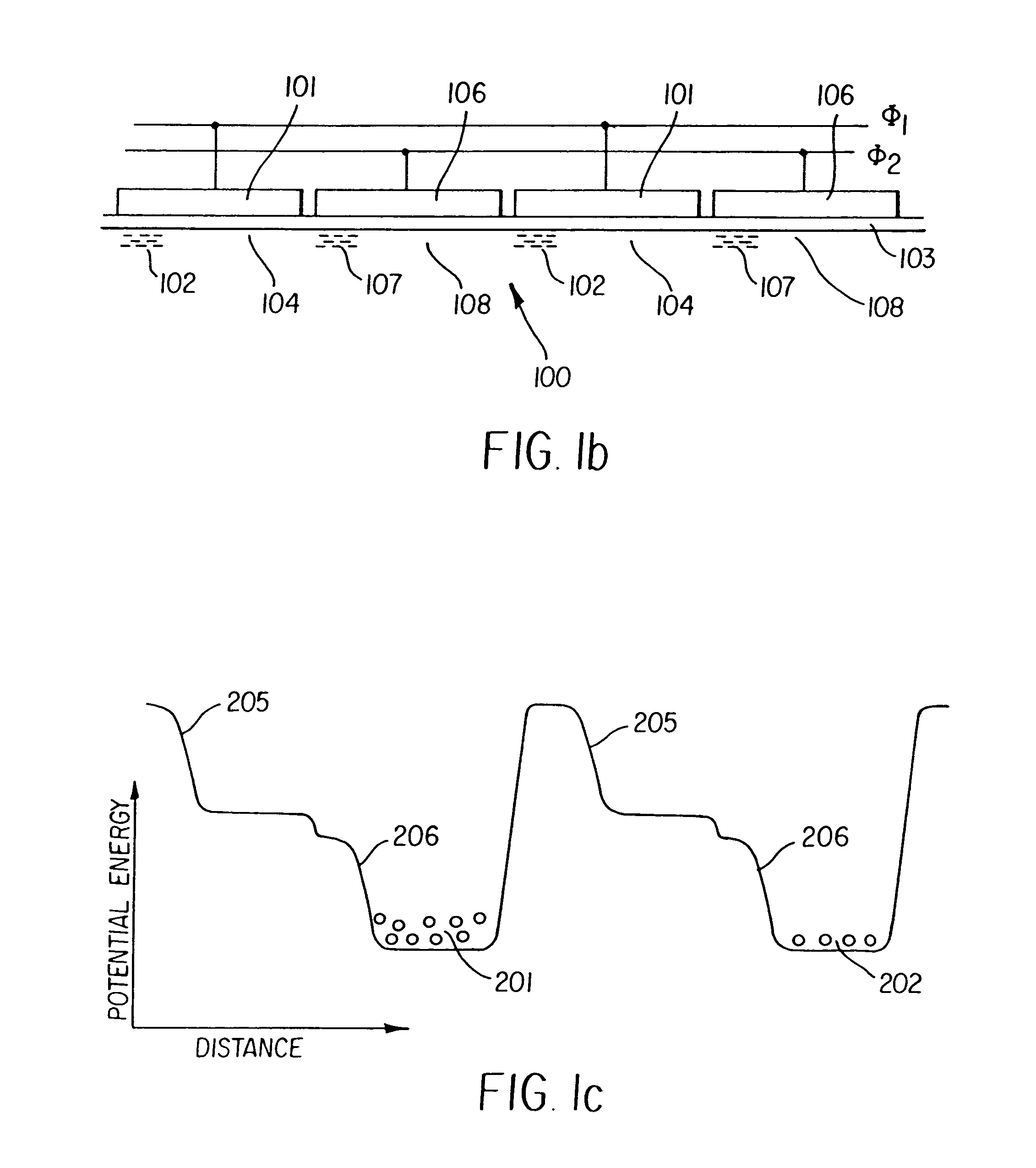
[0037]As discussed above, during the so-called accumulation mode clocking of the vertical shift register, one set of gates changes from a condition where holes are accumulated beneath the gate, at the Si—SiO2 interface, to a condition where the surface is depleted of holes. This results in excess hole charge being present which must be drained off. During the time required to drain off the excess hole charge, the p-well or substrate potential moves. This undesirable potential variation is referred to as p-well bounce. The present invention provides a means for maintaining accumulation mode clocking while avoiding the p-well bounce.

[0038]The fundamental problem that results in p-well bounce is that of disposal of the excess hole charges accumulated beneath one of the sets of gates of the CCD when that phase is switched out of accumulation and into depletion, and, conversely, the replenishment of the required hole charges when returning to the gates to accumulation. This problem becom...


PUM


Abstract

A method for reducing dark current within an image sensor includes applying, at a first time period, a first set of voltages to the phases of gate electrodes of vertical shift registers sufficient to accumulate holes of the vertical shift register, beneath each gate electrode and applying, at a second time period, a second voltage to a first set of the gate electrodes while simultaneously applying a more positive voltage to a second set of gate electrodes, the second voltage being of sufficient potential so holes that were accumulated beneath the second set of gate electrodes during the first time are collected and stored beneath the first set of gate electrodes during the second time period. Moreover, the method applies, at a third time period, a third voltage to the second set of gate electrodes while simultaneously applying a more positive voltage to the first set of gate electrodes, such that the previously accumulated holes beneath the first set of gate electrodes are transferred beneath the second set of gate electrodes; and returns the first and second sets of gate electrode voltages to their levels at the first time period.

Description

FIELD OF THE INVENTION[0001]The present invention relates to charge coupled devices (CCDs), and more particularly to reducing the level of dark current associated with these types of devices.BACKGROUND OF THE INVENTION[0002]Charge coupled devices (CCDs) that are used as image sensors are typically formed in lightly doped silicon materials. Light incident on the device and penetrating into the silicon produces electrons and holes in numbers proportional to the incident light intensity. The photogenerated electrons, having a higher mobility than the holes, are the preferred carrier to be collected and detected in such devices. These photogenerated electrons are transported in channels formed in lightly doped p-type silicon. Both, so-called, frame-transfer and interline transfer type CCD image sensing devices are typically fabricated in such lightly doped silicon. In interline transfer type devices and in some types of frame transfer type devices this is a lightly doped and relatively ...

Claims


Application Information

Patent Timeline
IPC IPC(8): H04N3/14G11C19/28H04N5/335H04N9/64H01L27/148H04N5/361
CPCH01L27/14806H04N5/361H01L27/14843H04N25/63
Inventor LOSEE, DAVID L.PARKS, CHRISTOPHER
Owner SEMICON COMPONENTS IND LLC
Why Eureka
Try Eureka