Minimization of FG-FG coupling in flash memory

a flash memory and fg-fg technology, applied in the field of flash memory technology, can solve the problems of prior art steps of fig. 6 for programming that do not compensate for fg—fg coupling, error during reading data from flash memory cells, etc., and achieve the effect of substantially eliminating the effect of fg—fg coupling

Active Publication Date: 2006-02-07
VALLEY DEVICE MANAGEMENT
View PDF6 Cites 139 Cited by
  • Summary
  • Abstract
  • Description
  • Claims
  • Application Information

AI Technical Summary

Benefits of technology

[0039]In this manner, first and second passes of the loop of program verify and programming steps are performed for compensating for FG—FG coupling. After the first pass of the loop of program verify and programming steps, the threshold voltage of a programmed flash memory cell reaches a value less than the program verify level. Subsequently, the second pass of the loop of program verify and programming steps is then performed for “fine-tuning” the threshold voltage to the program verify level. The amount of change to the threshold voltage for an adjacent flash memory cell from FG—FG coupling is proportional to the change in threshold voltage during programming of a flash memory cell. Because the change of threshold voltage during the second pass is relatively small, the effect of FG—FG coupling during the second pass is negligible. With performance of such multiple passes of program verify and programming steps, the effect of FG—FG coupling may be substantially eliminated during programming a page of a flash memory device.

Problems solved by technology

Unfortunately, the prior art does not compensate for such undesired FG—FG coupling during programming of a flash memory device. FIG. 6 shows a flow-chart of steps for programming a group of flash memory cells in a page.
The prior art steps of FIG. 6 for programming do not compensate for FG—FG coupling between adjacent flash memory cells.
Such undesired change in the threshold voltage of a flash memory cells from FG—FG coupling may result in error during reading of data from the flash memory cell.

Method used


Image

  • Minimization of FG-FG coupling in flash memory
  • Minimization of FG-FG coupling in flash memory
  • Minimization of FG-FG coupling in flash memory

Examples


Embodiment Construction

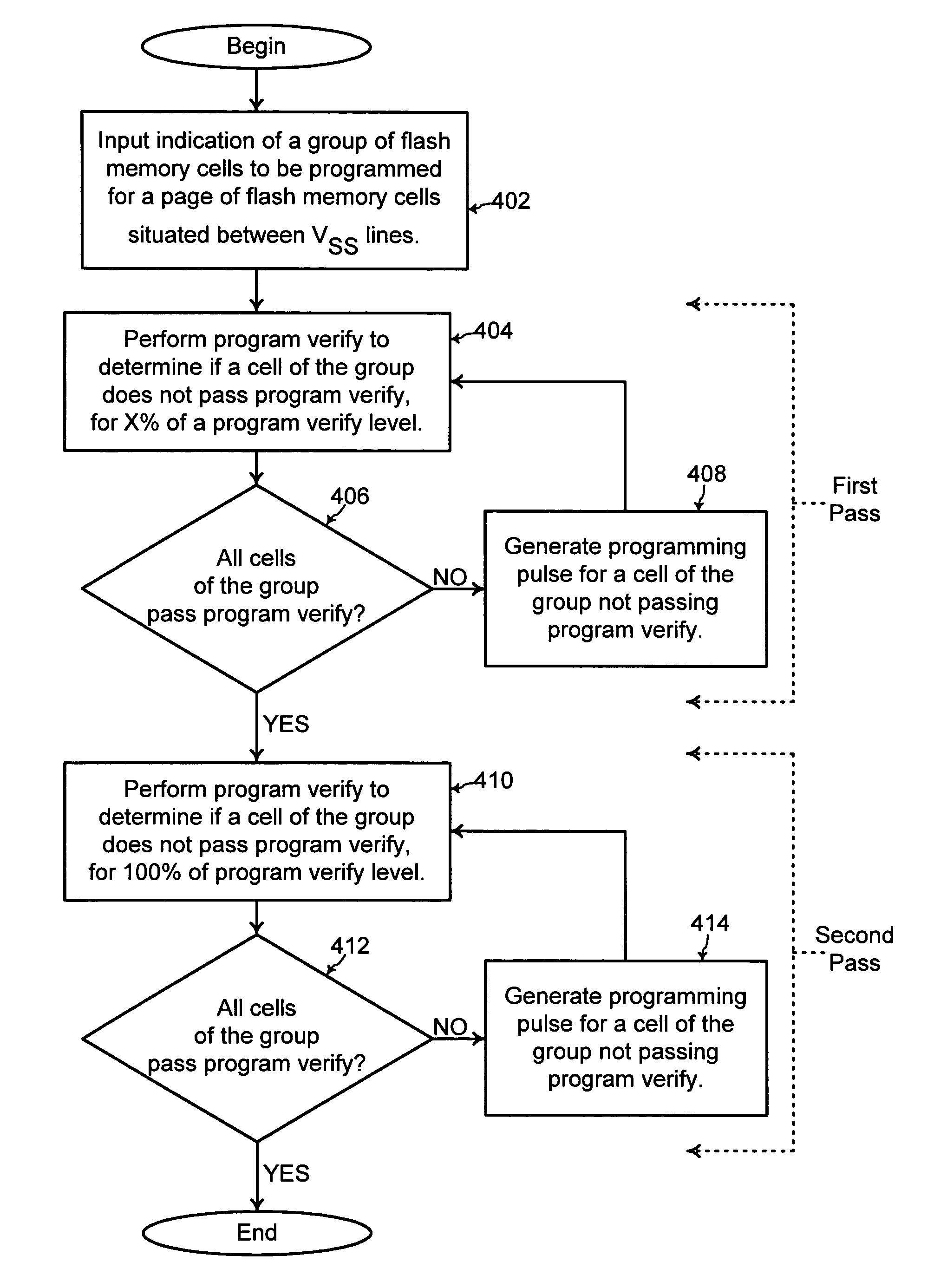
[0051]FIG. 7 shows a block diagram of a system 300 for programming the array of flash memory cells 130 with compensation for FG—FG coupling. The system 300 includes a program circuitry 302 for generating programming voltages to be applied on a flash memory cell to be programmed. In addition, an X-decoder 304 and a Y-decoder 306 are coupled between the program circuitry 302, the array of flash memory cells 130, and an address sequencer 308.

[0052]The address sequencer 308 provides the address bits for a flash memory cell in the array 130 to be programmed. The X-decoder 304 and the Y-decoder 306 decode the address bits from the address sequencer 308 to couple the programming voltages from the program circuitry 302 on the word-line and the bit-line, respectively, for the flash memory cell to be programmed.

[0053]A read / verify circuitry 310 generates reading voltages used for reading the programmed or erased state of a flash memory cell. The X-decoder 304 and the Y-decoder 306 decode the ...


PUM


Abstract

Multiple passes of the loop of program verify and programming steps are performed for minimizing the effects of FG—FG coupling during programming a flash memory device. In one embodiment of the present invention, for programming a group of at least one flash memory cell of an array, a first pass of program verify and programming steps is performed until each flash memory cell of the group attains a threshold voltage that is at least X % of a program verify level but less than the program verify level. Then, a second pass of program verify and programming steps are performed until each flash memory cell of the group attains substantially the program verify level for the threshold voltage.

Description

TECHNICAL FIELD[0001]The present invention relates generally to flash memory technology, and more particularly, to a method and system for minimizing FG—FG (floating gate to floating gate) coupling during programming.BACKGROUND OF THE INVENTION[0002]Referring to FIG. 1, a flash memory cell 100 of a flash memory device includes a tunnel dielectric structure 102 typically comprised of silicon dioxide (SiO2) or nitrided oxide as known to one of ordinary skill in the art of integrated circuit fabrication. The tunnel dielectric structure 102 is disposed on a semiconductor substrate or a p-well 103. In addition, a floating gate structure 104, comprised of a conductive material such as polysilicon for example, is disposed over the tunnel dielectric structure102. A control dielectric structure 106, typically comprised of silicon dioxide (SiO2) and silicon nitride (Si3N4), such as an ONO (oxide-nitride-oxide) structure for example, is disposed over the floating gate structure 104. A control ...

Claims


Application Information

Patent Timeline
Patent Type & Authority Patents(United States)
IPC IPC(8): G11C16/04
CPCG11C16/0416G11C16/0466G11C16/3459G11C16/3427G11C16/3418
Inventor FASTOW, RICHARDPARK, SHEUNGHEE
Owner VALLEY DEVICE MANAGEMENT
Why Eureka
Try Eureka