Polishing apparatus and a method of polishing and cleaning and drying a wafer

a technology of polishing apparatus and wafer, which is applied in the direction of lighting and heating apparatus, lapping machines, heating types, etc., can solve the problems of difficult to remove contaminants by cleaning, conventional polishing apparatus cannot be placed in a clean room, and the surface of the polished wafer is generally quite contaminated with semiconductor material particles and abrasives

Inactive Publication Date: 2006-02-14
EBARA CORP +1
View PDF25 Cites 14 Cited by
  • Summary
  • Abstract
  • Description
  • Claims
  • Application Information

AI Technical Summary

Benefits of technology

[0012]It is therefore an object of the present invention to provide a polishing apparatus which can be installed in a clean room and does not contaminate the ambient atmosphere in the clean room, and whi

Problems solved by technology

The surface of the semiconductor wafer which has been polished is generally quite contaminated not only with particles of semiconductor material but also with abrasive material.
The conventional polishing apparatus could not be placed in a clean room because of the dust particles generated by the polishing apparatus itself.
Once the contaminants which adhere to

Method used


Image

  • Polishing apparatus and a method of polishing and cleaning and drying a wafer
  • Polishing apparatus and a method of polishing and cleaning and drying a wafer
  • Polishing apparatus and a method of polishing and cleaning and drying a wafer

Examples


first embodiment

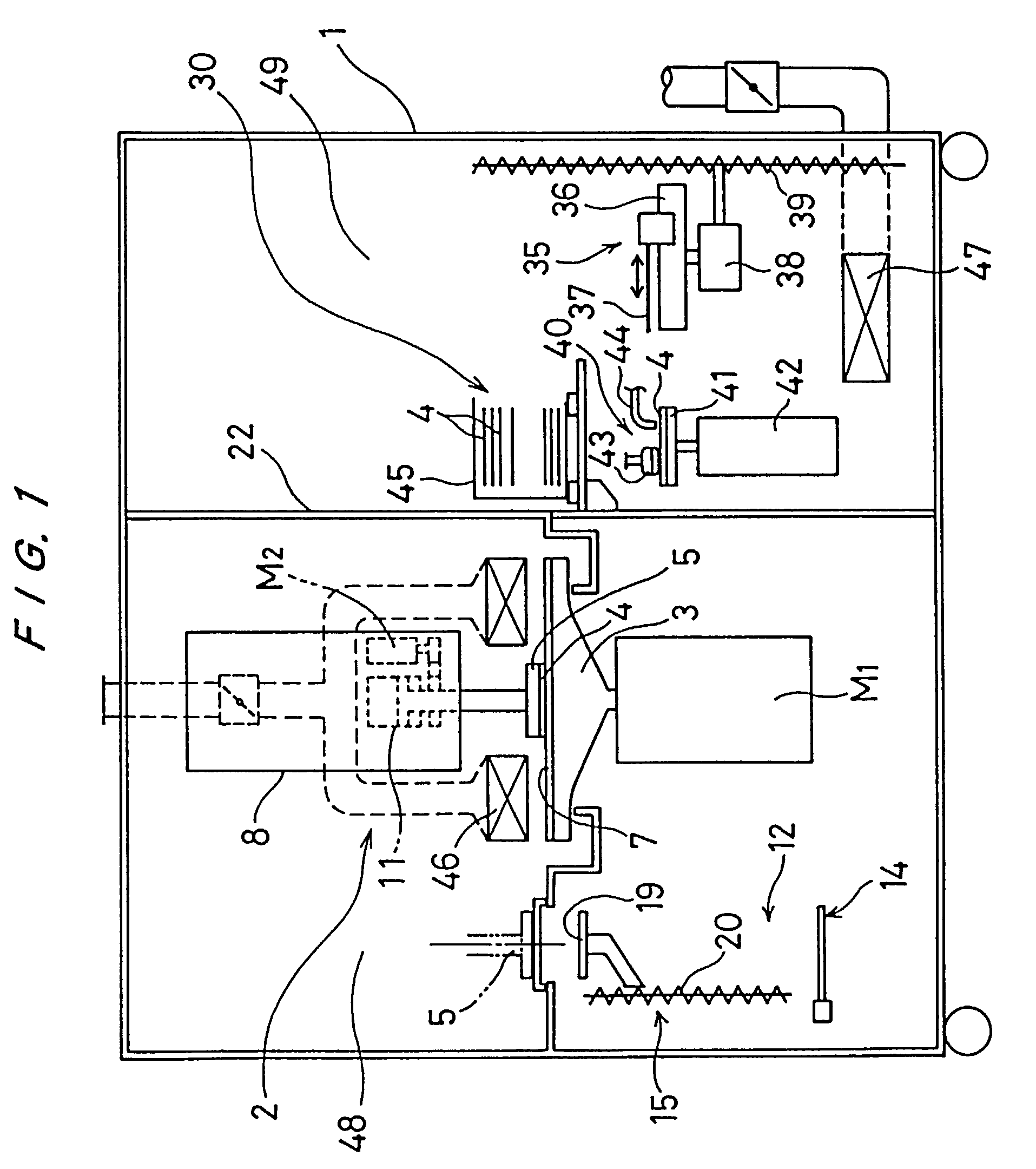
[0031]A polishing apparatus according to the present invention will be described below with reference to FIGS. 1 and 2.

[0032]As shown in FIGS. 1 and 2, a polishing apparatus has a housing unit 1 with side walls, a top wall and a bottom wall housing a polishing section 2 for polishing semiconductor wafers and a cleaning section 30 for cleaning the semiconductor wafers which have been polished. The interior of the housing unit 1 is partitioned by a partition wall 22 into a first chamber 48 and a second chamber 49. The polishing section 2 is disposed in the first chamber 48, and the cleaning section 30 is disposed in the second chamber 49.

[0033]The polishing section 2 comprises a turntable 3 and a top ring 5 for holding a semiconductor wafer 4 and pressing the semiconductor wafer 4 against the turntable 3. The turntable 3 is coupled to a motor M1. An abrasive cloth 7 is attached to an upper surface of the turntable 3. The top ring 5 is coupled to a top ring head 8 which is provided wit...

second embodiment

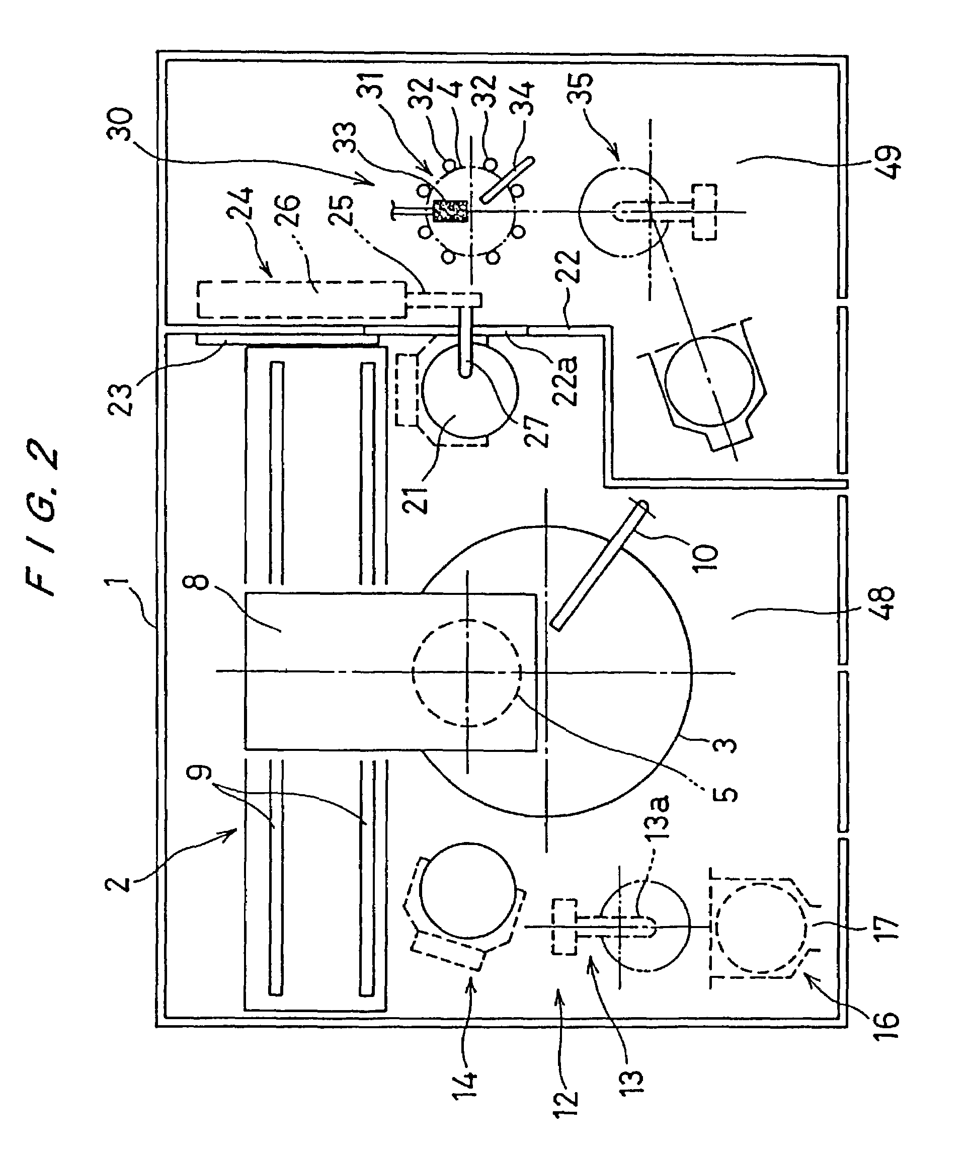
[0057]A polishing apparatus according to the present invention will be described below with reference to FIGS. 3 through 8.

[0058]FIG. 3 is a perspective view of a polishing apparatus 50 which is installed in a clean room. A wall 53 with a side wall 53A partitions the clean room into a working zone 54 of a high degree of cleanliness and a utility zone 55 of a low degree of cleanliness. The side wall 53A is provided with a cassette delivery opening 51 and an operator panel 52. The polishing apparatus 50 is an enclosed structure by a housing unit comprising the side walls 53A, 53B and a ceiling 53C, and houses a load / unload section for delivering a cassette which stores a plurality of semiconductor wafers, a transfer section for transferring the semiconductor wafers, a polishing section for polishing semiconductor wafers, a cleaning unit for cleaning the semiconductor wafers which have been polished, and a control unit for controlling the operation of the overall apparatus. All of the ...

third embodiment

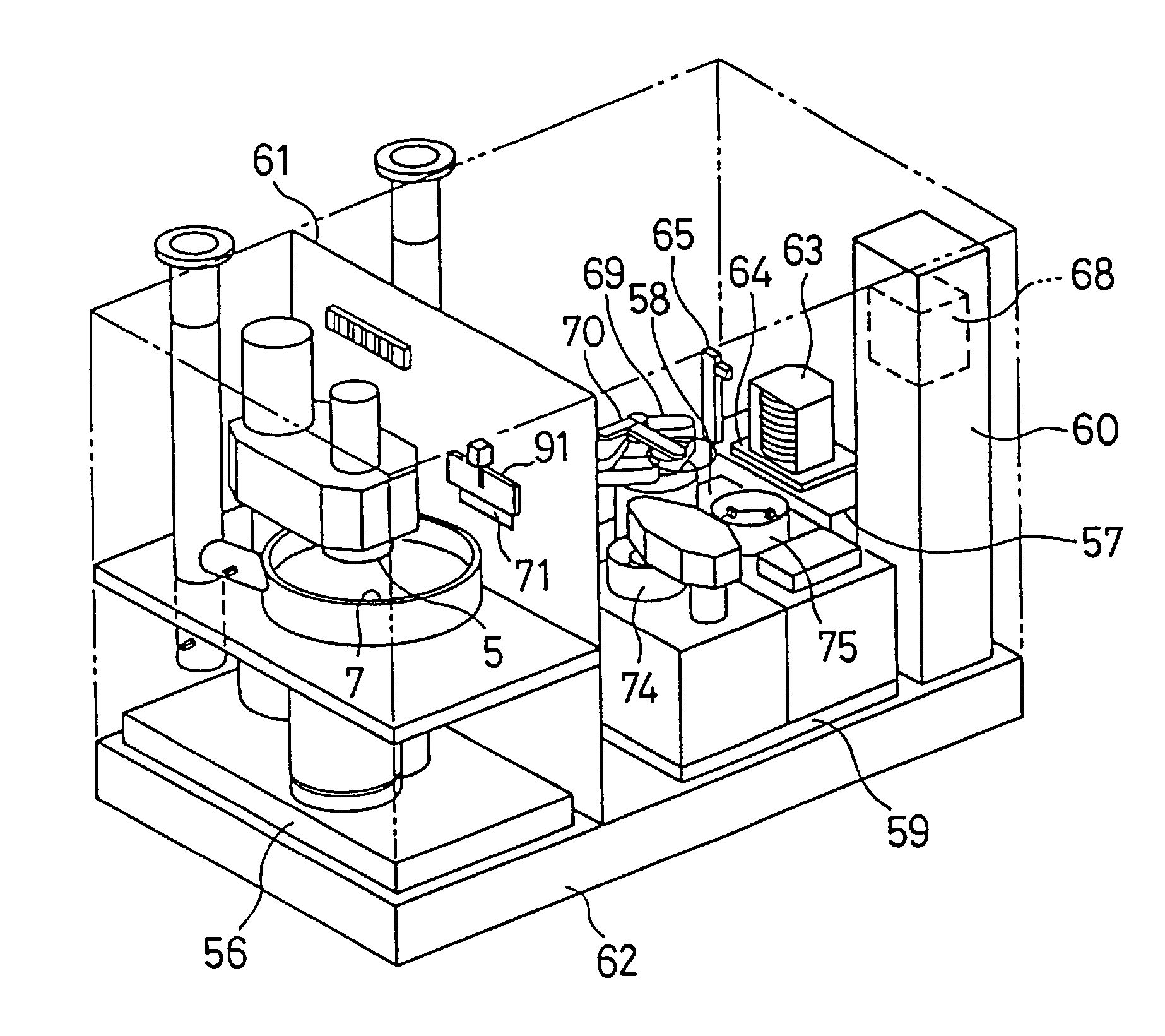
[0088]A polishing apparatus according to the present invention will be described below with reference to FIGS. 9 and 10.

[0089]The polishing apparatus in FIGS. 9 and 10 is identical to the polishing apparatus in FIGS. 3 through 5 with the exception that a filtering unit 100 is provided on the ceiling 53C. Those parts shown in FIGS. 9 and 10 which are identical to those shown in FIGS. 3 through 5 are denoted by identical reference numerals, and will not be described in detail below.

[0090]As shown in FIG. 9, above the ceiling 53C, there is provided a filtering unit 100 for circulating clean air through the second chamber 76 housing the load / unload section 57, the transfer section 58 and the cleaning section 59.

[0091]FIG. 10 is a side view of the interior of the polishing apparatus 50. The polishing apparatus 50 is divided by the partition wall 61 into a first chamber 77 having the polishing section 56, and a second chamber 76 having the load / unload section 57, the transfer section 58, ...


PUM

PropertyMeasurementUnit
Internal pressureaaaaaaaaaa

Abstract

A polishing apparatus for polishing a surface of a workpiece includes a housing unit, a partition wall partitioning an interior of the housing unit into a first chamber and a second chamber, a polishing section disposed in the first chamber and having a turntable with an abrasive cloth mounted on an upper surface thereof and a top ring positioned above the turntable for supporting the workpiece to be polished and pressing the workpiece against the abrasive cloth, and a cleaning section disposed in the second chamber and cleaning the workpiece which has been polished. The polishing apparatus further includes a transferring device for transferring the workpiece which has been polished from the polishing section to the cleaning section through an opening and an exhaust system for exhausting ambient air from each of the polishing section and cleaning section separately and independently.

Description

[0001]This is a continuation of application Ser. No. 08 / 884,410, filed Jun. 27, 1997, and now U.S. Pat. No. 6,500,051, issued Dec. 31, 2002, which is a continuation of application Ser. No. 08 / 563,295, filed Nov. 28, 1995, and now U.S. Pat. No. 5,679,059.BACKGROUND OF THE INVENTION[0002]1. Field of the Invention[0003]The present invention relates to a polishing apparatus, and more particularly to a polishing apparatus having a polishing section for polishing a workpiece such as a semiconductor wafer to a flat mirror finish and a cleaning section for cleaning the workpiece which has been polished.[0004]2. Description of the Related Art[0005]Recent rapid progress in semiconductor device integration demands smaller and smaller wiring patterns or interconnections and also narrower spaces between interconnections which connect active areas. One of the processes available for forming such interconnection is photolithography. Though the photolithographic process can form interconnections th...

Claims


Application Information

Patent Timeline
IPC IPC(8): B24B1/00H01L21/304B08B1/04B24B27/00B24B37/34B24B51/00B24B55/12F24F3/16H01L21/00
CPCB08B1/04B08B15/02B24B27/0023B24B37/345B24B51/00H01L21/67219F24F3/161H01L21/67017H01L21/67028H01L21/67057B24B55/12F24F3/167H01L21/304
Inventor NISHI, TOYOMITOGAWA, TETSUJISAITO, HARUMITSUTSUJIMURA, MANABUYAJIMA, HIROMIHIMUKAI, KAZUAKIKODAMA, SHOICHIIMOTO, YUKIOAOKI, RIICHIROWATASE, MASAKOSHIGETA, ATSUSHIMISHIMA, SHIROKOUNO, GISUKE
Owner EBARA CORP
Why Eureka
Try Eureka