

Mask for manufacturing a highly-integrated circuit device
a technology of integrated circuit and mask, which is applied in the direction of photomechanical equipment, instruments, originals for photomechanical treatment, etc., can solve the problems of inability to achieve the desired reduction of the depth of focus (dof), the inability to reduce the line width of the remaining interconnection structure connecting the remaining gates, and the inability to achieve the desired reduction of the line width of the interconnection
Inactive Publication Date: 2006-02-14
SAMSUNG ELECTRONICS CO LTD
View PDF2 Cites 0 Cited by
- Summary
- Abstract
- Description
- Claims
- Application Information
AI Technical Summary
Benefits of technology
[0009]To solve the above-described problems, the present invention provides, among other things, a set of masks capable of substantially reducing the line width of interconnections of a highly-integrated circuit device.
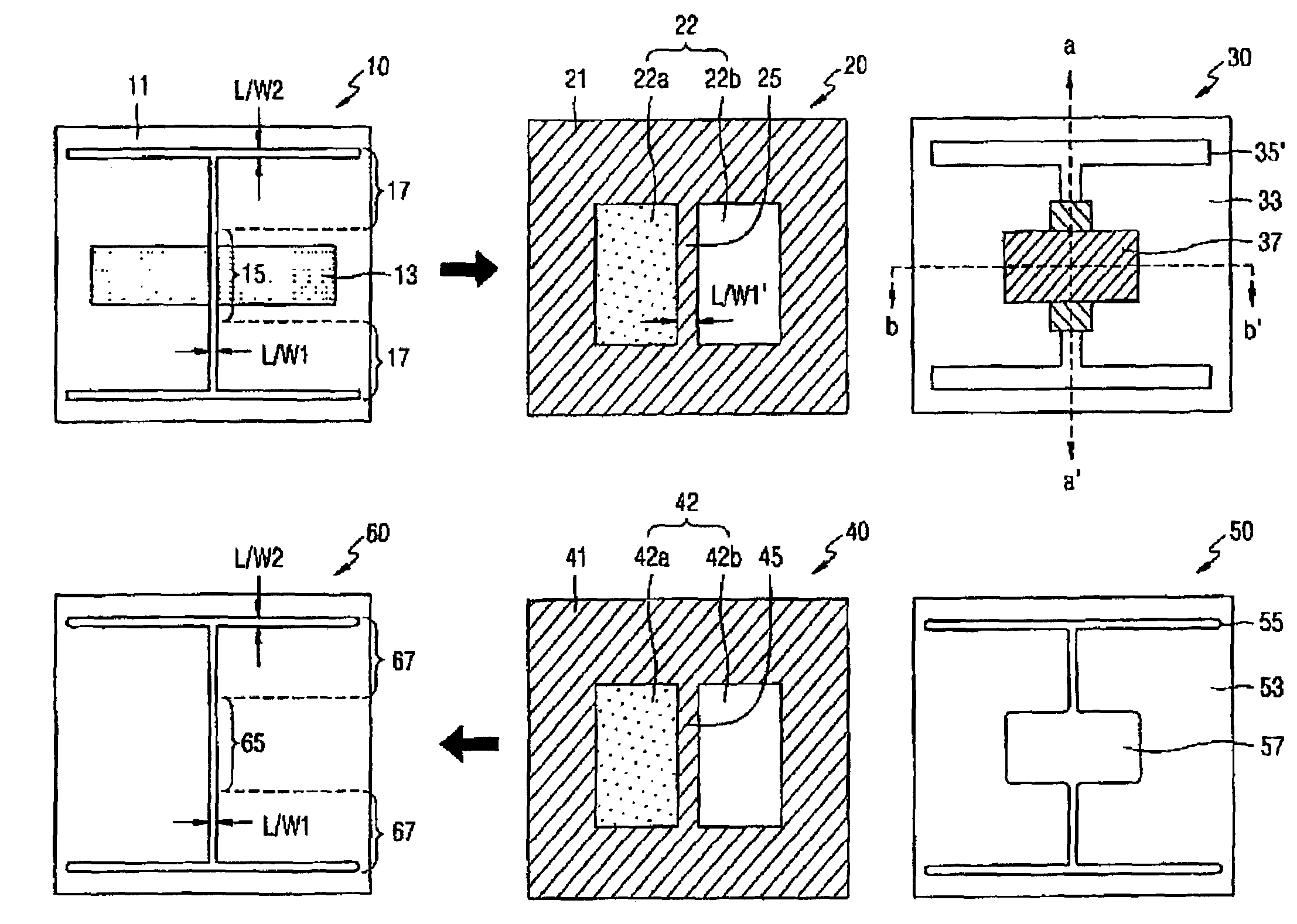
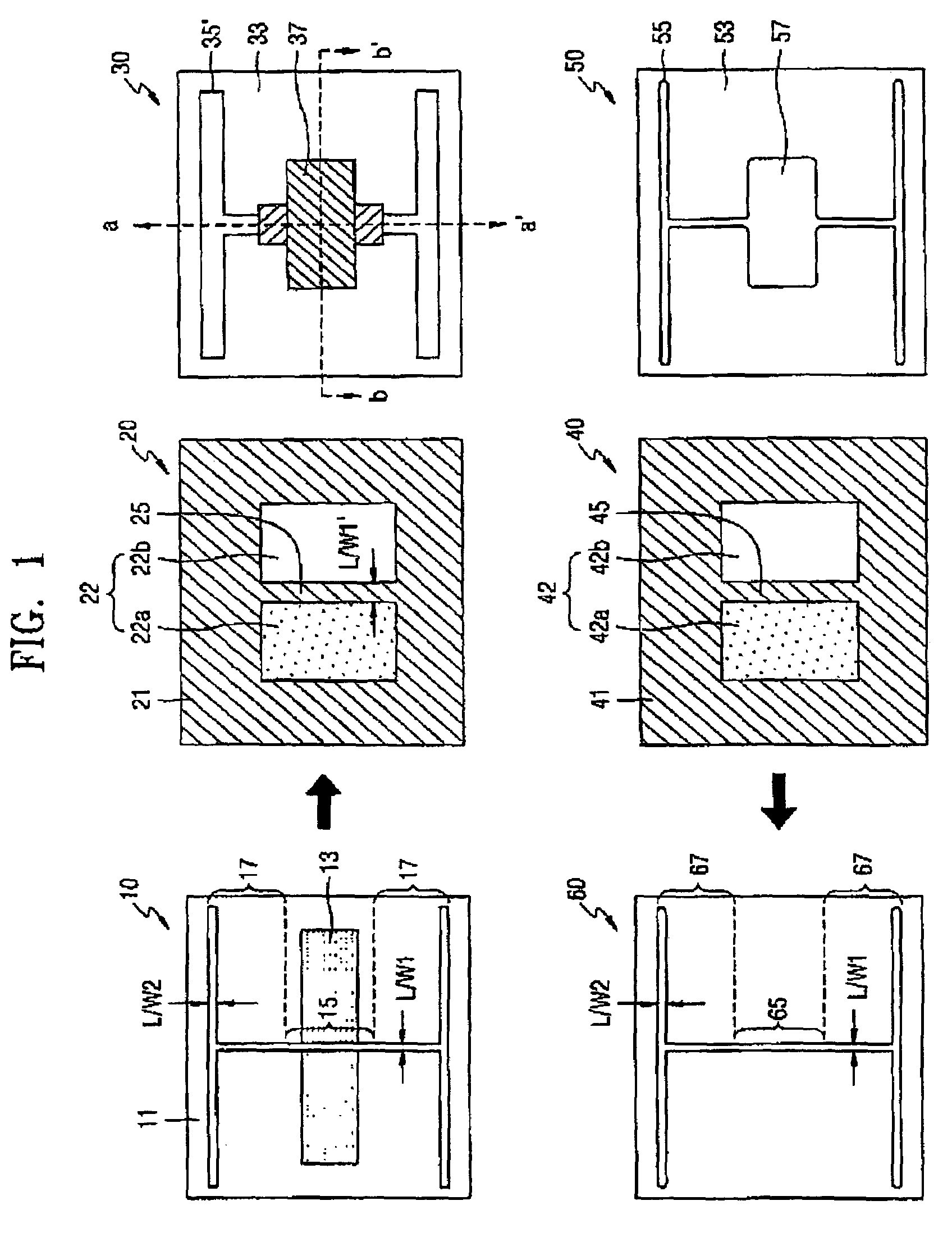
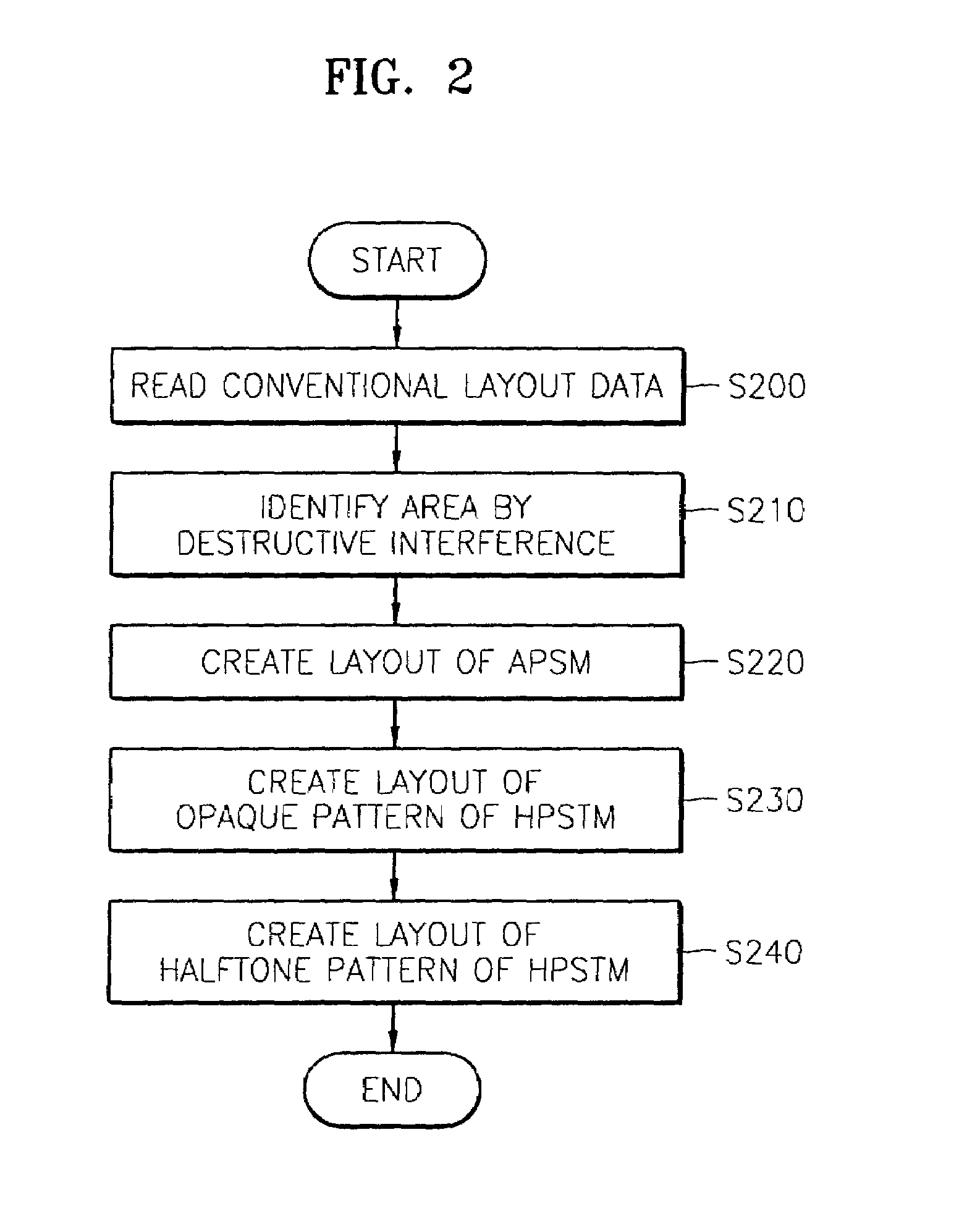
[0016]According to another aspect of the present invention, a method of creating a layout of a set of masks is provided. After reading the layout data of an interconnection line having a large line width, an area in which an access interconnection line is formed to have a line width smaller than the large line width by destructive interference is identified from the read layout data. Next, a layout of an APSM having first and second phase shifting areas is created based on the identification. The first and second phase shifting areas have different phases and are disposed adjacent to each other to generate destructive interference. Finally, a layout of a HPSTM having an opaque pattern and a halftone pattern is created. The opaque pattern prevents the access interconnection line defined by the APSM from being erased. The halftone pattern defines a pass interconnection line, which has a line width smaller than the large line width, and is connected to the access interconnection line.
Problems solved by technology
However, the smaller the size of the pattern, the less resolution the pattern has due to optical proximity effects between adjacent patterns.
If the numerical aperture is increased to increase the resolution of an optical apparatus, the depth of focus (DOF) is undesirably decreased.
But the line width of the remaining interconnection structures connecting the remaining gates has not been reduced as desired.
Therefore, it is difficult to form the highly-integrated device on a small chip area using the prior art techniques.
Method used
View moreImage
Smart ImageViewing Examples

Examples
experimental example 1
[0075]A mask image of the APSM 20 (FIG. 1) in which the opaque line pattern 25 has a line width L / W1′ of 0.36 μm and a mask image of the HPSTM 30 (FIG. 1) in which the halftone pattern 35 has a line width L / W_Ht of 0.48 μm were simulated, as shown in FIG. 9A. The APSM 20 and the HPSTM 30 were simulated, provided that a ¼ scale-down stepper adapting an exposure source having a wavelength of 248 nm was used. As a result, a HPSTM image 50 and a final image 60 were obtained. In the final image 60, a line width L / W1 of an access gate was 0.09 μm, and a line width L / W2 of a pass gate was 0.11 μm. Accordingly, it is understood that both the access gate image and the pass gate image were well formed.
Login to View More PUM
 Abstract
A set of masks including an alternating phase shifting mask (APSM) and a halftone phase shifting trim mask (HPSTM) is provided. The APSM includes first and second phase shifting areas and a first opaque pattern. The first and second phase shifting areas are disposed adjacent to each other and have different phases for generating destructive interference. Further, the first and second phase shifting areas define an access interconnection line. The first opaque pattern is formed on a transparent substrate to define the first and second phase shifting areas. The HPSTM includes a second opaque pattern on the transparent substrate and a halftone pattern. The second opaque pattern prevents an access interconnection line from being erased. The halftone pattern defines a pass interconnection line connected to the access interconnection line.
Description
BACKGROUND OF THE INVENTION[0001]This application claims priority from Korean Patent Application No. 2002-51194, filed Aug. 28, 2002, which is incorporated herein in its entirety by reference.[0002]1. Field of the Invention[0003]The present invention relates to masks for manufacturing a highly-integrated circuit device, a method of creating a layout of the mask, a method of manufacturing the mask and a method of manufacturing the highly-integrated circuit device using the mask.[0004]2. Description of the Related Art[0005]As the integration density of semiconductor devices increases, design rules are scaled down into the deep submicron range and under. However, the smaller the size of the pattern, the less resolution the pattern has due to optical proximity effects between adjacent patterns.[0006]If the numerical aperture is increased to increase the resolution of an optical apparatus, the depth of focus (DOF) is undesirably decreased. Thus, a phase shift mask (PSM) for shifting and ...
Claims
Login to View More Application Information
Patent Timeline
 IPC IPC(8): G03F1/08G06F17/50G03F1/30G03F1/32G03F1/68G03F1/70G03F7/20H01L21/027
CPCG03F1/144G03F7/70466G03F1/0061G03F1/32G03F1/30G03F1/70H01L21/027
InventorPARK, CHUL-HONGYOO, MOON-HYUNKIM, YOO-HYONKIM, DONG-HYUNCHOI, SOO-HAN
OwnerSAMSUNG ELECTRONICS CO LTD