X-ray imaging device
- Summary
- Abstract
- Description
- Claims
- Application Information
AI Technical Summary
Benefits of technology
Problems solved by technology
Method used
Image
Examples
first embodiment
(First Embodiment)
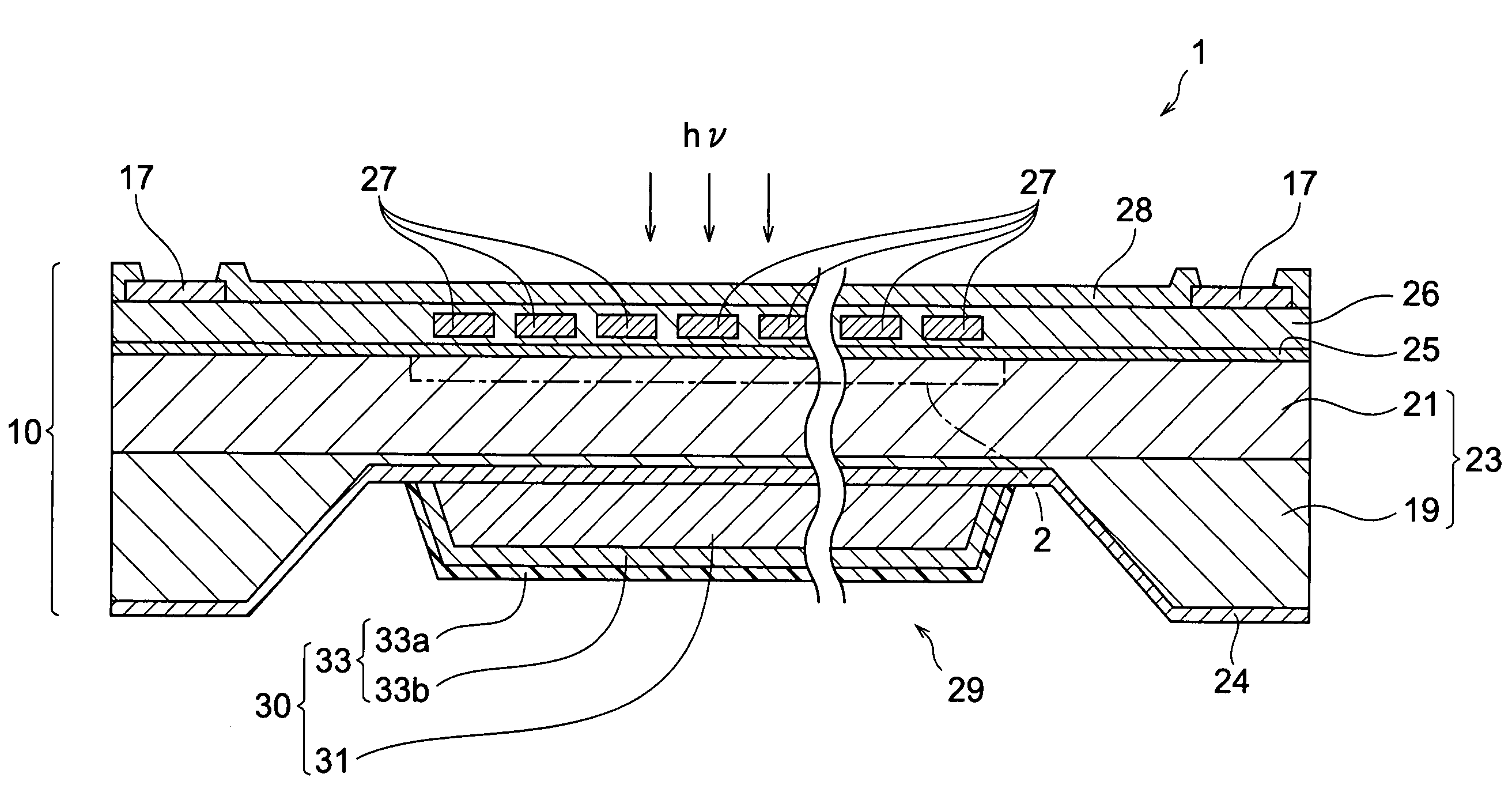
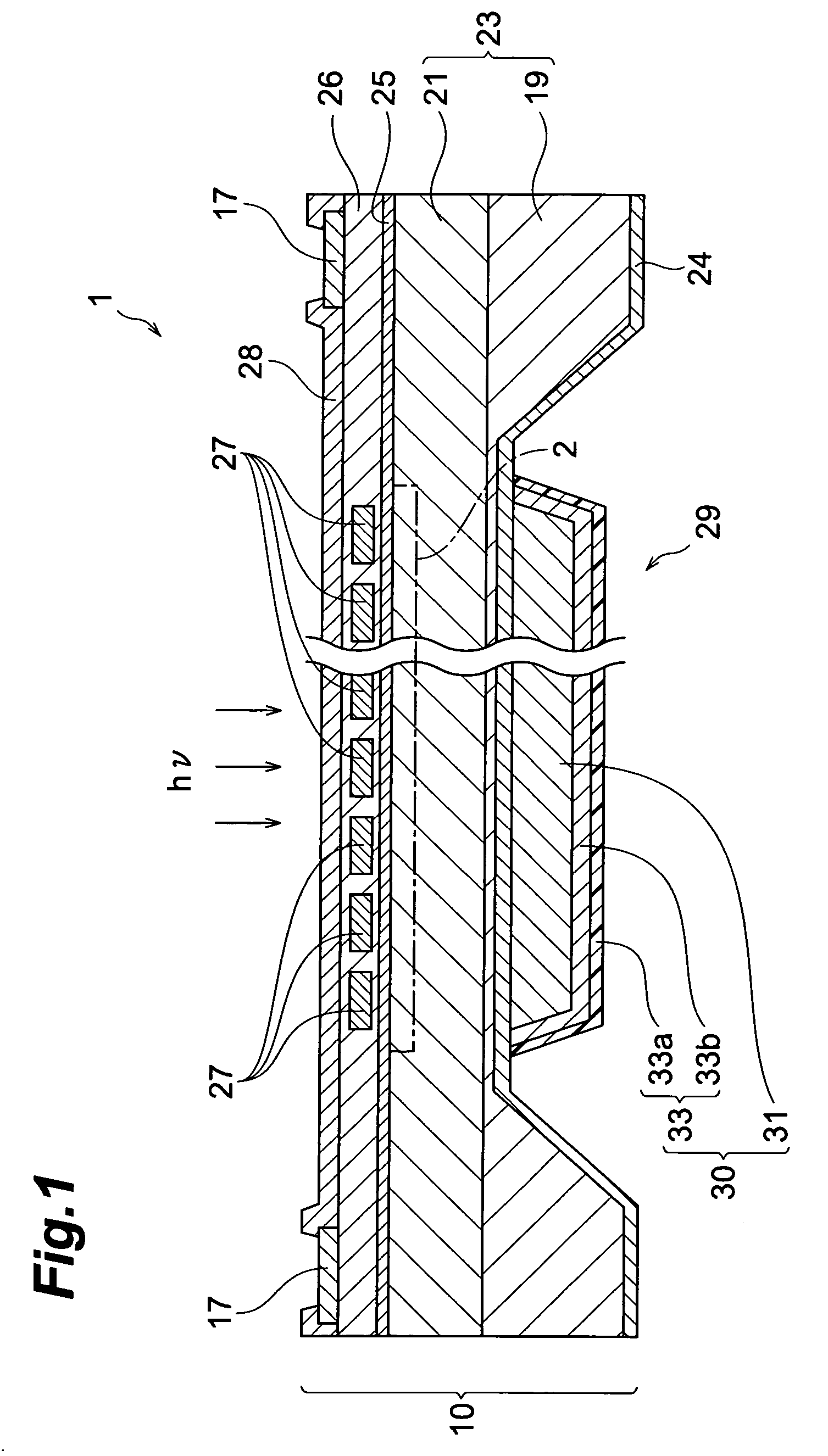
[0031]FIG. 1 is a schematic depiction of a sectional structure of the X-ray imaging device in accordance with a first embodiment. In the description hereinafter, the front surface refers to the surface of X-ray incidence (that is, the upper surface in FIG. 1), and the rear surface refers to the opposite surface (that is, the lower surface in FIG. 1) to the front surface. The X-ray imaging device 1 is provided with a CCD portion 10 and a scintillation portion 30.
[0032]The CCD portion 10 has a semiconductor substrate 23. The semiconductor substrate 23 includes a high concentration p+-type semiconductor layer 19 and a p-type epitaxial layer 21 deposited on p+-type semiconductor layer 19. An insulating layer 25 is provided on the semiconductor substrate 23 (the p-type epitaxial layer 21). A plurality of transfer electrodes 27 made of polysilicon are provided in an insulating layer 26 on the insulating layer 25. An insulating layer 28 and electrode pads 17 (described be...
second embodiment
(Second Embodiment)
[0051]FIG. 4 is a schematic representation of a sectional structure of the X-ray imaging device in accordance with a second embodiment. Hereinafter, the surface of X-ray incidence (the lower surface in FIG. 4) refers to the rear surface, and the opposite surface (the upper surface in FIG. 4) to the surface of X-ray incidence refers to the front surface.
[0052]As shown in FIG. 4, an X-ray imaging device 51 is provided with the CCD portion 10 and the scintillation portion 30. The CCD portion 10 has the semiconductor substrate 23. The Semiconductor substrate 23 includes the p+-type semiconductor layer 19 and the p-type epitaxial layer 21.
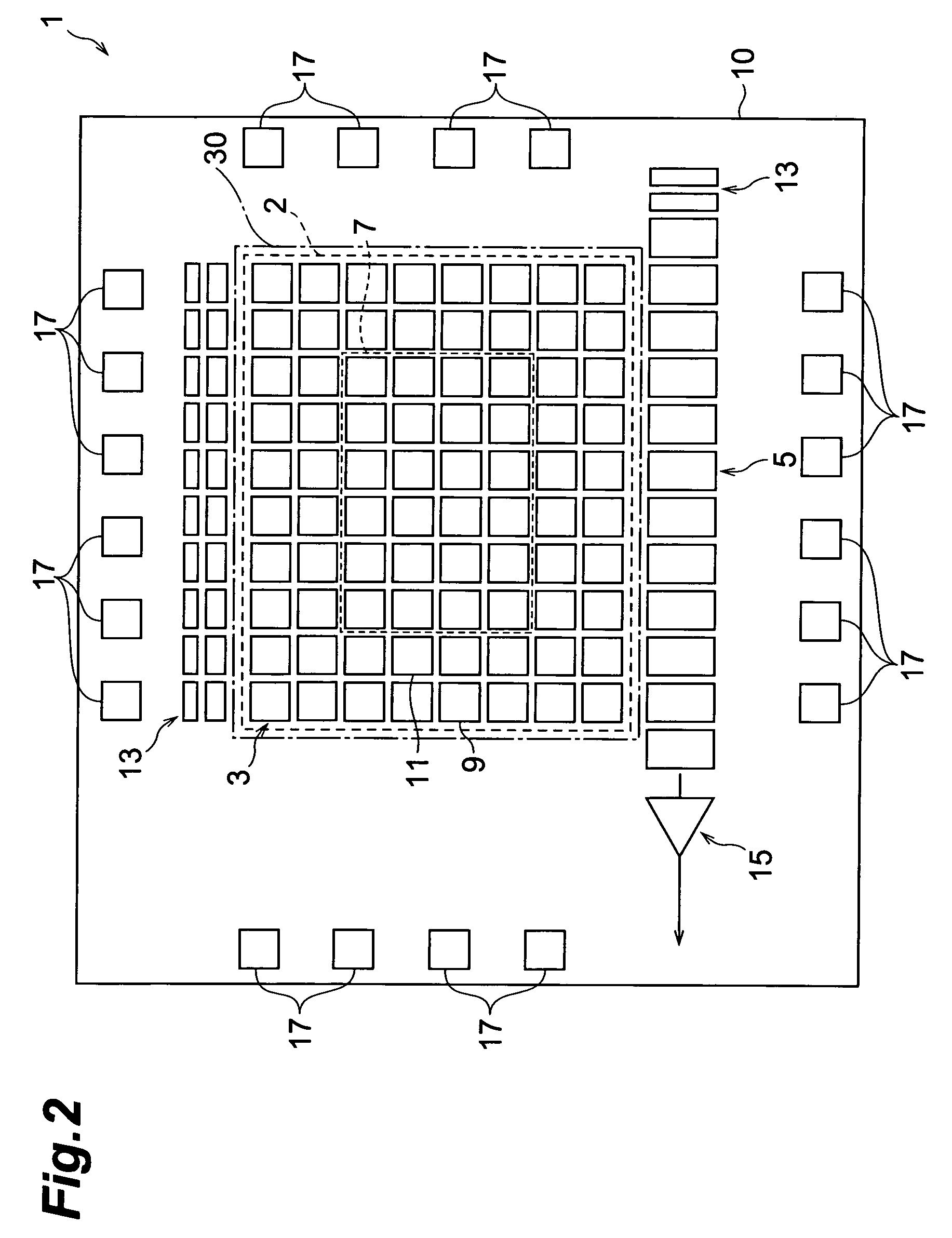
[0053]It is noted that the CCD portion 10 has the vertical shift register portion 3 and the horizontal shift register portion 5 as shown in FIG. 2. The imaging portion 2 includes the photo detecting area 7, the optical black area 9 and the isolation area 11.
[0054]The scintillation portion 30 is arranged on the insulating layer 28 so a...
PUM
 Abstract
Description
Claims
Application Information
 - R&D
- Intellectual Property
- Life Sciences
- Materials
- Tech Scout
- Unparalleled Data Quality
- Higher Quality Content
- 60% Fewer Hallucinations
Browse by: Latest US Patents, China's latest patents, Technical Efficacy Thesaurus, Application Domain, Technology Topic, Popular Technical Reports.
© 2025 PatSnap. All rights reserved.Legal|Privacy policy|Modern Slavery Act Transparency Statement|Sitemap|About US| Contact US: help@patsnap.com


