Method of manufacturing twin-ONO-type SONOS memory using reverse self-alignment process

a sonos memory and reverse self-alignment technology, applied in the direction of semiconductor devices, electrical equipment, transistors, etc., can solve the problems of deteriorating the endurance of sonos, the complexity of the patterning structure in which the floating gate and the control gate are stacked, and the photolithographic and etching process for forming hyperfine devices is about to reach the technical limits, so as to achieve stable 2-bit characteristics

Active Publication Date: 2006-02-28
SAMSUNG ELECTRONICS CO LTD
View PDF12 Cites 48 Cited by
  • Summary
  • Abstract
  • Description
  • Claims
  • Application Information

AI Technical Summary

Benefits of technology

[0054]According to the present invention, even if the linewidth of a memory gate is reduced to 0.10 μm or less, a SONOS memory with stable 2-bit characteristics can be manufactured.

Problems solved by technology

Nonvolatile semiconductor memory devices can not only electrically erase and program data but also retain data even during interruption of power supply.
Although conventional stack-gate-type nonvolatile memory cells have been constantly scaled down, photolithographic and etching processes for forming hyperfine devices are about to reach the technical limits.
That is, in addition to scaling vows, patterning a structure in which a floating gate and a control gate are stacked becomes complicated due to a high step difference or a high aspect ratio.
The accumulated charges may deteriorate the SONOS endurance.
Similarly, after hole charges are programmed, accumulated holes may make the endurance of the device poor.
Although there is a possibility that the distribution of electrons or holes in an ONO dielectric layer can be minimally adjusted by optimization of process conditions or by appropriate control of driving voltage, shorter and shorter gate lengths cannot assure the 2-bit characteristics anymore.

Method used


Image

  • Method of manufacturing twin-ONO-type SONOS memory using reverse self-alignment process
  • Method of manufacturing twin-ONO-type SONOS memory using reverse self-alignment process
  • Method of manufacturing twin-ONO-type SONOS memory using reverse self-alignment process

Examples


embodiment 1

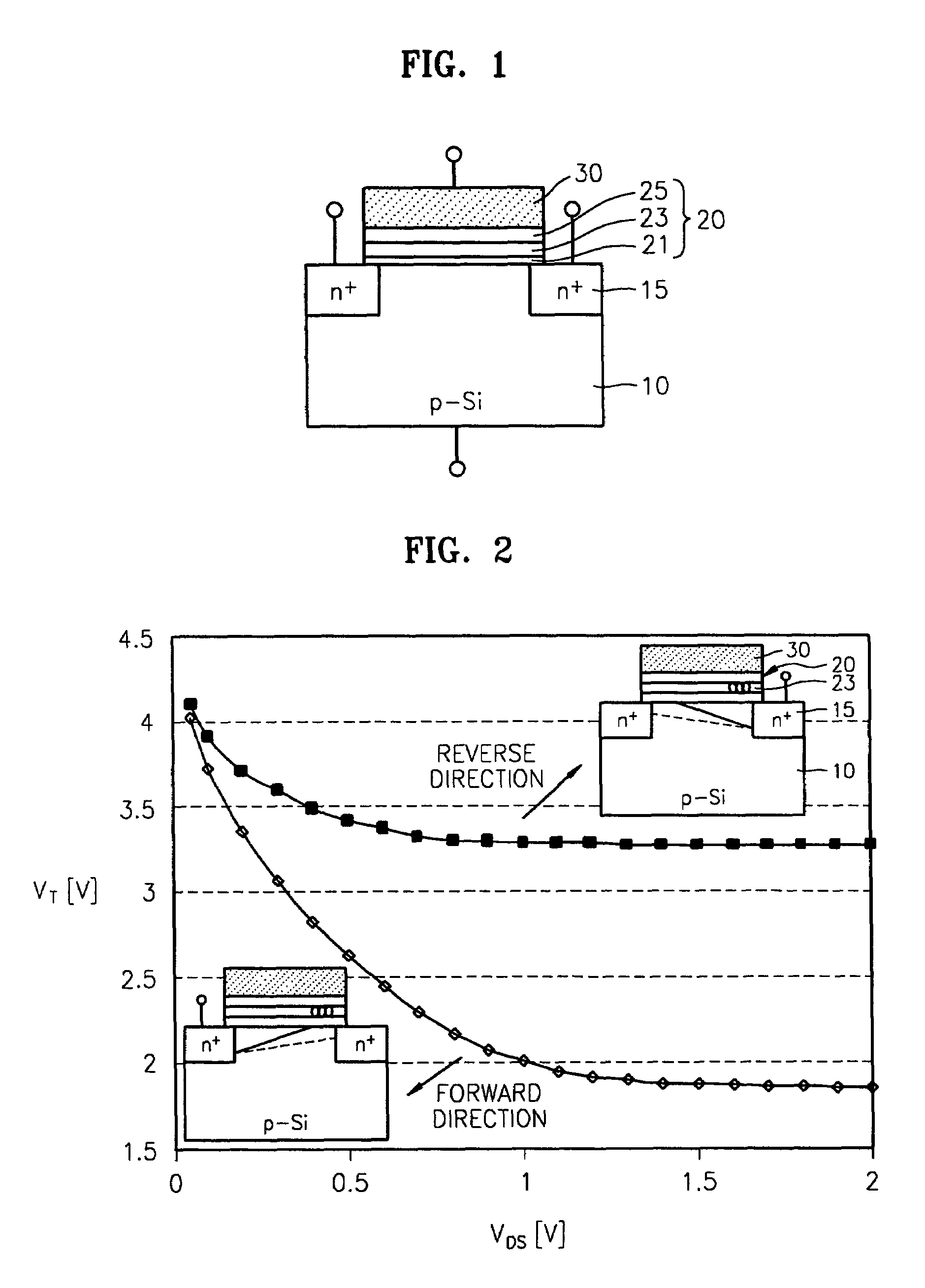
[0073] a Twin-ONO-type SONOS with a Single Gate

first embodiment

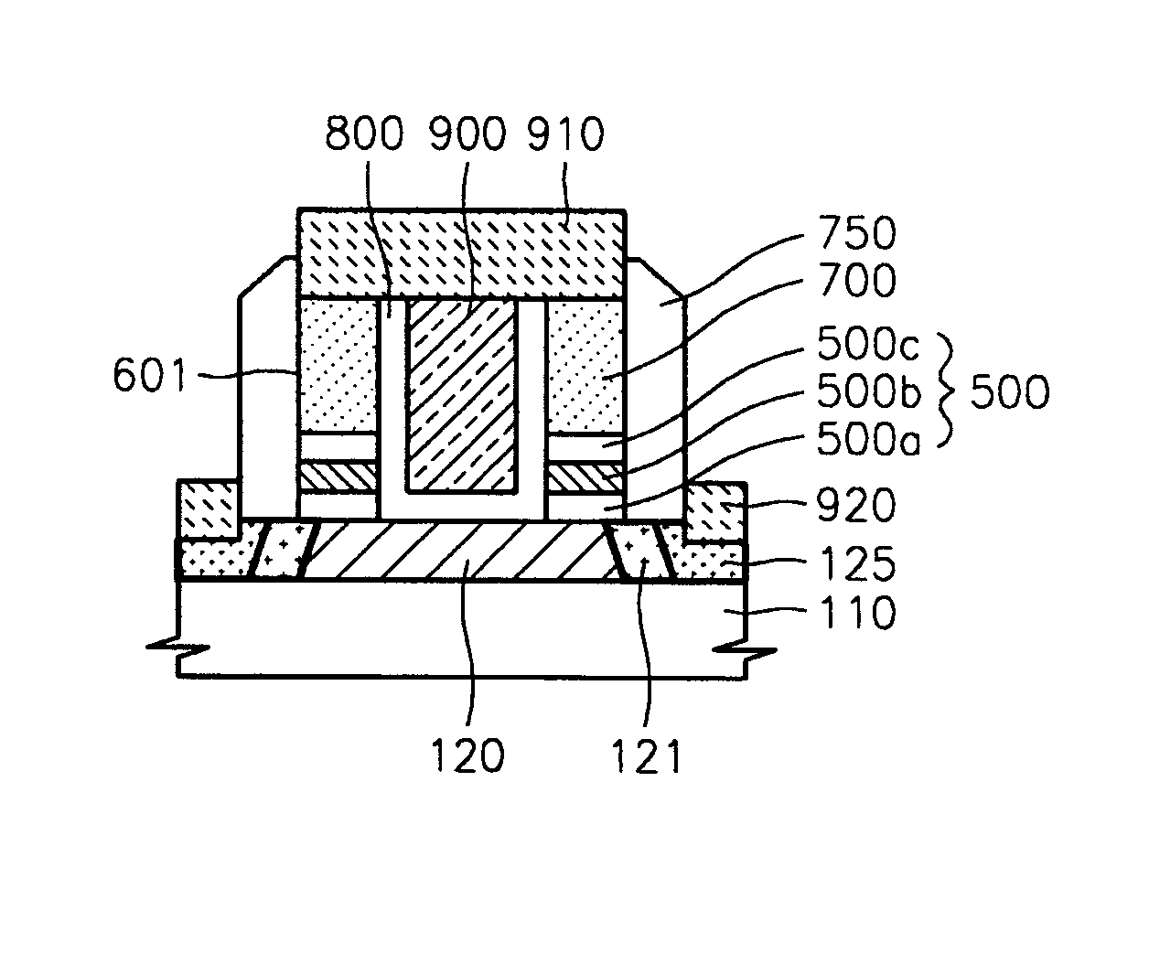
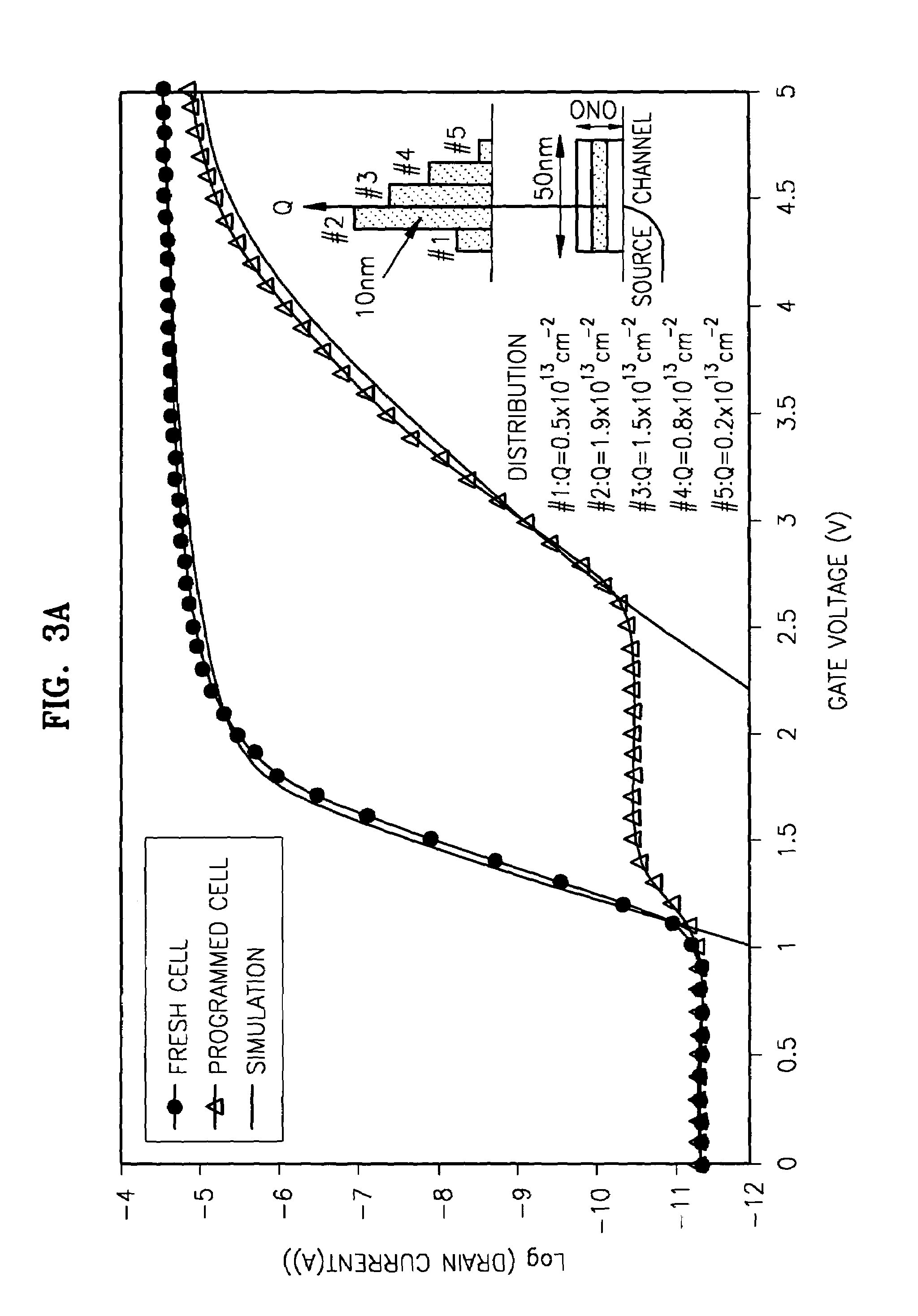
[0074]FIGS. 5A through 5K are schematic cross-sectional views illustrating a twin-ONO-type SONOS memory according to the present invention.

[0075]Referring to FIG. 5A, as a starting material for manufacturing a SONOS memory, a p-type substrate is prepared. For example, as shown in FIG. 5A, a silicon (120)-on-insulator (110) (SOI) substrate is prepared. Here, the SOI substrate exhibits p-type conductivity and serves as a p-type substrate. However, a typical bulk silicon substrate may be substituted for the SOI substrate. Afterwards, a field region is formed using a device isolation technique on the silicon layer 120, to define an active region. The device isolation technique may be, for example, a shallow trench isolation, a self-aligned shallow trench isolation, or a LOCOS.

[0076]Referring to FIG. 5B, an oxide-silicon-oxide (ONO) dielectric layer 500 is formed on a Si channel region of the silicon layer 120. The ONO dielectric layer 500 can be formed by a known method and substantiall...

embodiment 2

[0091] a Twin-ONO-type SONOS with 3 Gates

[0092]The second embodiment, unlike the first embodiment, deals with a triple-gate-type SONOS memory device. The same reference numerals in the first and second embodiments represent the same element.


PUM


Abstract

A method of manufacturing a twin-ONO-type SONOS memory using a reverse self-alignment process, wherein an ONO dielectric layer is formed under a gate and physically separated into two portions using a reverse self-alignment process irrespective of photolithographic limits. To facilitate the reverse self-alignment, a buffer layer and spacers for defining the width of the ONO dielectric layer are adopted. Thus, the dispersion of trapped charges during programming and erasing can be appropriately adjusted, thus improving the characteristics of the SONOS. The present invention prevents the redistribution of charges in time after the programming and erasing operations.

Description

BACKGROUND OF THE INVENTION[0001]1. Field of the Invention[0002]The present invention relates to a method of manufacturing a semiconductor memory device. More particularly, the present invention is directed to a method of manufacturing a twin-ONO-type SONOS memory device, which can function as a 2-bit operating memory device with asymmetric programming, using a reverse self-alignment process.[0003]2. Description of the Related Art[0004]In recent years, nonvolatile semiconductor memory devices have been used in various applications. Nonvolatile semiconductor memory devices can not only electrically erase and program data but also retain data even during interruption of power supply. An example of a nonvolatile semiconductor memory device is a flash memory cell.[0005]Conventionally, stack-gate-type flash memories, in which floating gates and control gates are stacked, have been developed and produced in mass. Floating gates are intended for programming charges, and control gates are i...

Claims


Application Information

Patent Timeline
Patent Type & Authority Patents(United States)
IPC IPC(8): H01L21/336H01L21/8247H01L21/28H01L27/115H01L29/423H01L29/788H01L29/792
CPCH01L21/28282H01L29/7923H01L29/66833H01L29/40117H10B69/00
Inventor LEE, YONG-KYUHAN, JEONG-UKKANG, SUNG-TAEGLEE, JONG-DUKPARK, BYUNG-GOOK
Owner SAMSUNG ELECTRONICS CO LTD
Why Eureka
Try Eureka