Method for fabricating a microelectronic circuit including applying metal over and thickening the integrated coil to increase conductivity

a microelectronic circuit and integrated coil technology, applied in the field of microelectronic circuits, can solve the problems of poor quality factor of the integrated semiconductor element having the conductive element, poor inherent conductivity poor quality factor of the electrically conductive element, etc., to achieve the effect of reducing impedance, reducing impedance, and ensuring the same conductivity

Inactive Publication Date: 2006-02-28
INFINEON TECH AG
View PDF12 Cites 4 Cited by
  • Summary
  • Abstract
  • Description
  • Claims
  • Application Information

AI Technical Summary

Benefits of technology

[0018]The method according to the invention thickens an already existing electrically conductive, monolithically integrated coil in a finished processed microelectronic circuit with a metal which has the same conductivity as, or a higher conductivity than, the metal of the monolithically integrated coil. By virtue of this thickening of the monolithically integrated coil, more conductive material is applied on interconnects of the monolithically integrated coil by comparison with the unthickened state, and this leads to a reduced impedance by comparison with the unthickened state. The reduction of the impedance is accompanied by a corresponding increase in the conductivity of the affected monolithically integrated coil of the microelectronic circuit.
[0019]Consequently, the invention advantageously achieves an improved quality factor of the electrically conductive element of a microelectronic circuit.
[0020]A further advantage of the method according to the invention is that the method follows the fabrication of an already finished processed microelectronic circuit.

Problems solved by technology

One problem with such electrically conductive elements known from the prior art is that their inherent conductivity is relatively low.
This requires special operating conditions, such as e.g. low temperatures, or, under defined operating conditions, e.g. at defined temperatures, leads to a poor quality factor of the electrically conductive element.
This in turn leads to a poor quality factor of the integrated semiconductor element having the conductive element.

Method used


Image

  • Method for fabricating a microelectronic circuit including applying metal over and thickening the integrated coil to increase conductivity
  • Method for fabricating a microelectronic circuit including applying metal over and thickening the integrated coil to increase conductivity
  • Method for fabricating a microelectronic circuit including applying metal over and thickening the integrated coil to increase conductivity

Examples


Embodiment Construction

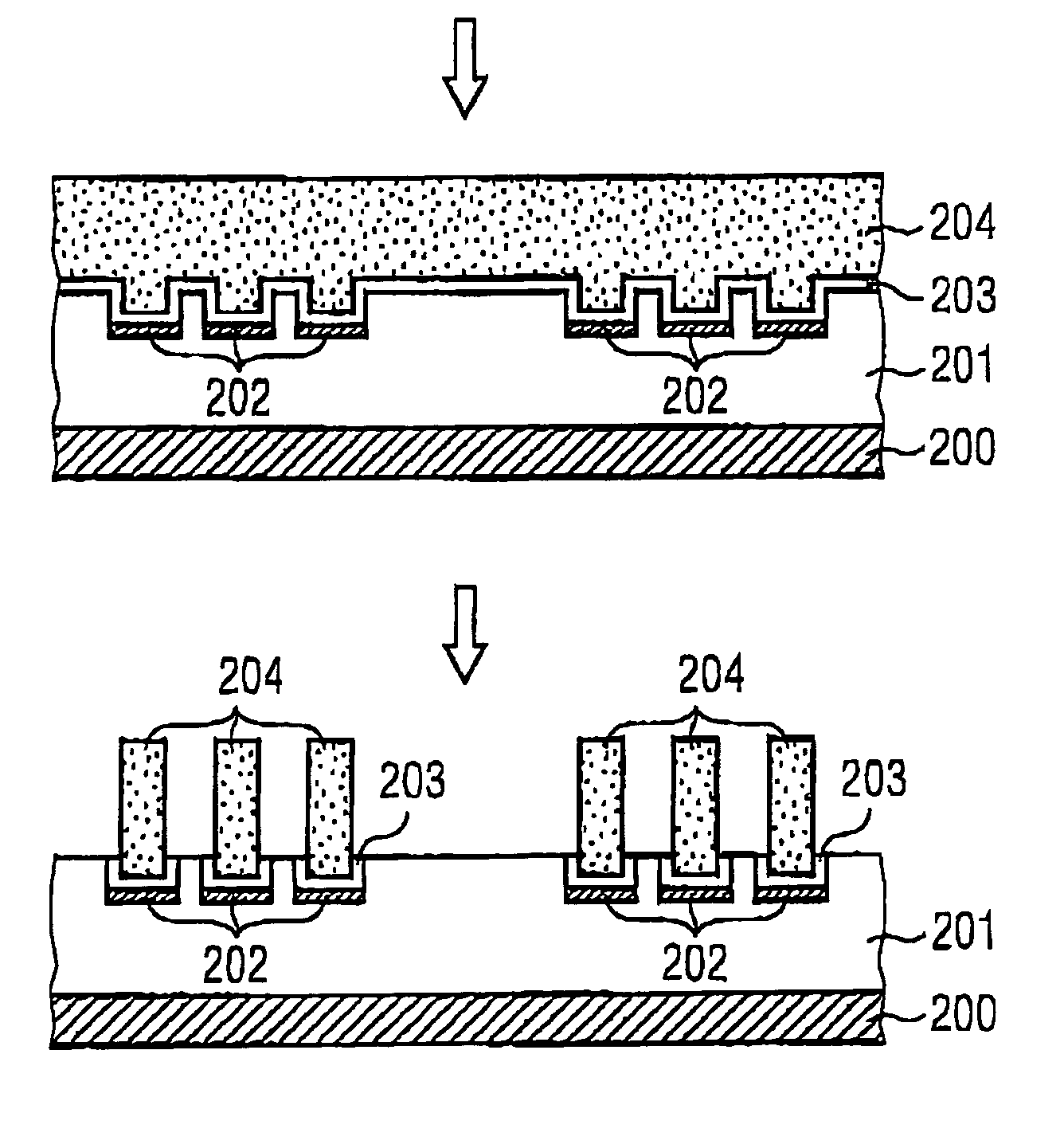
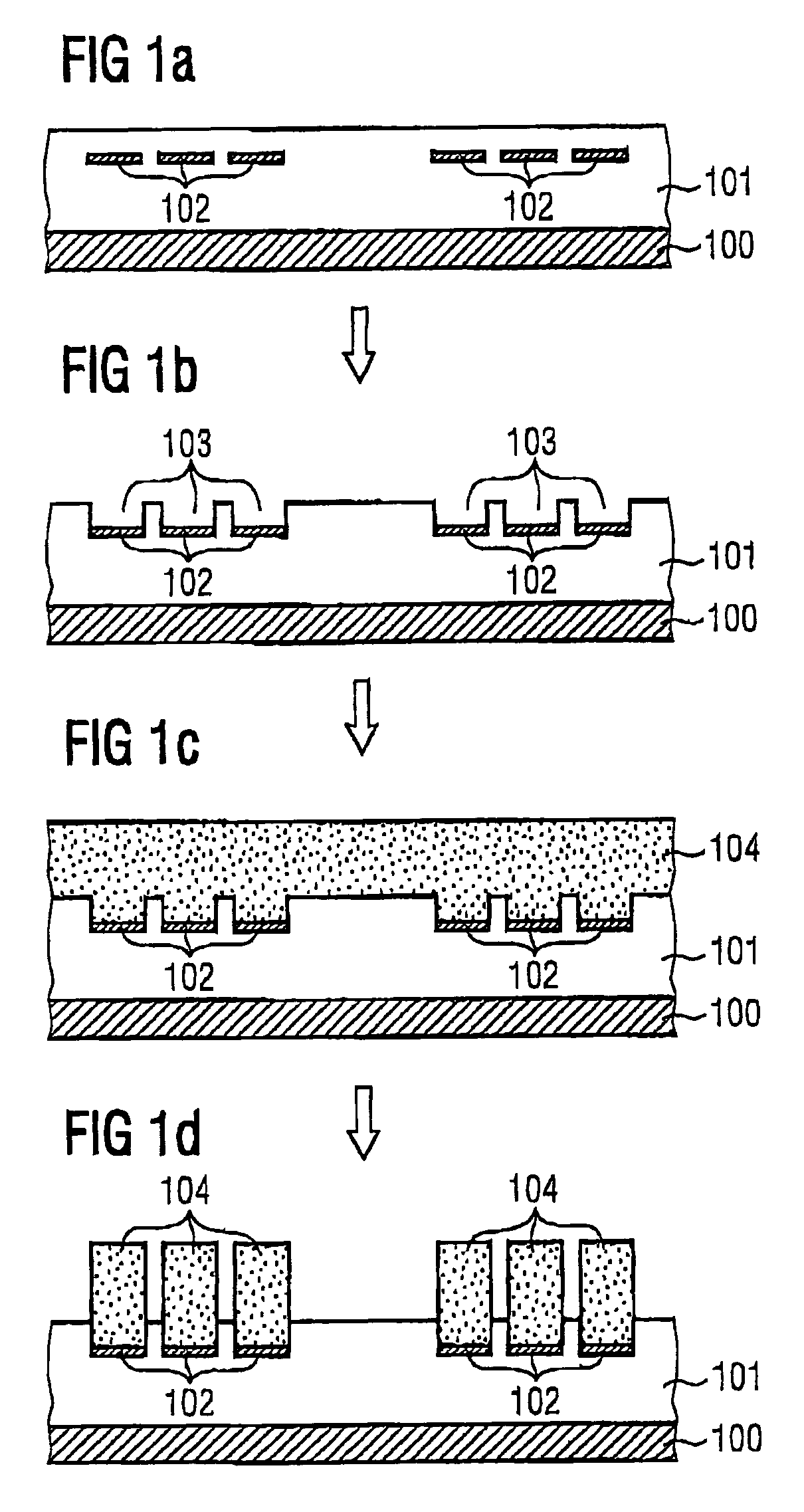
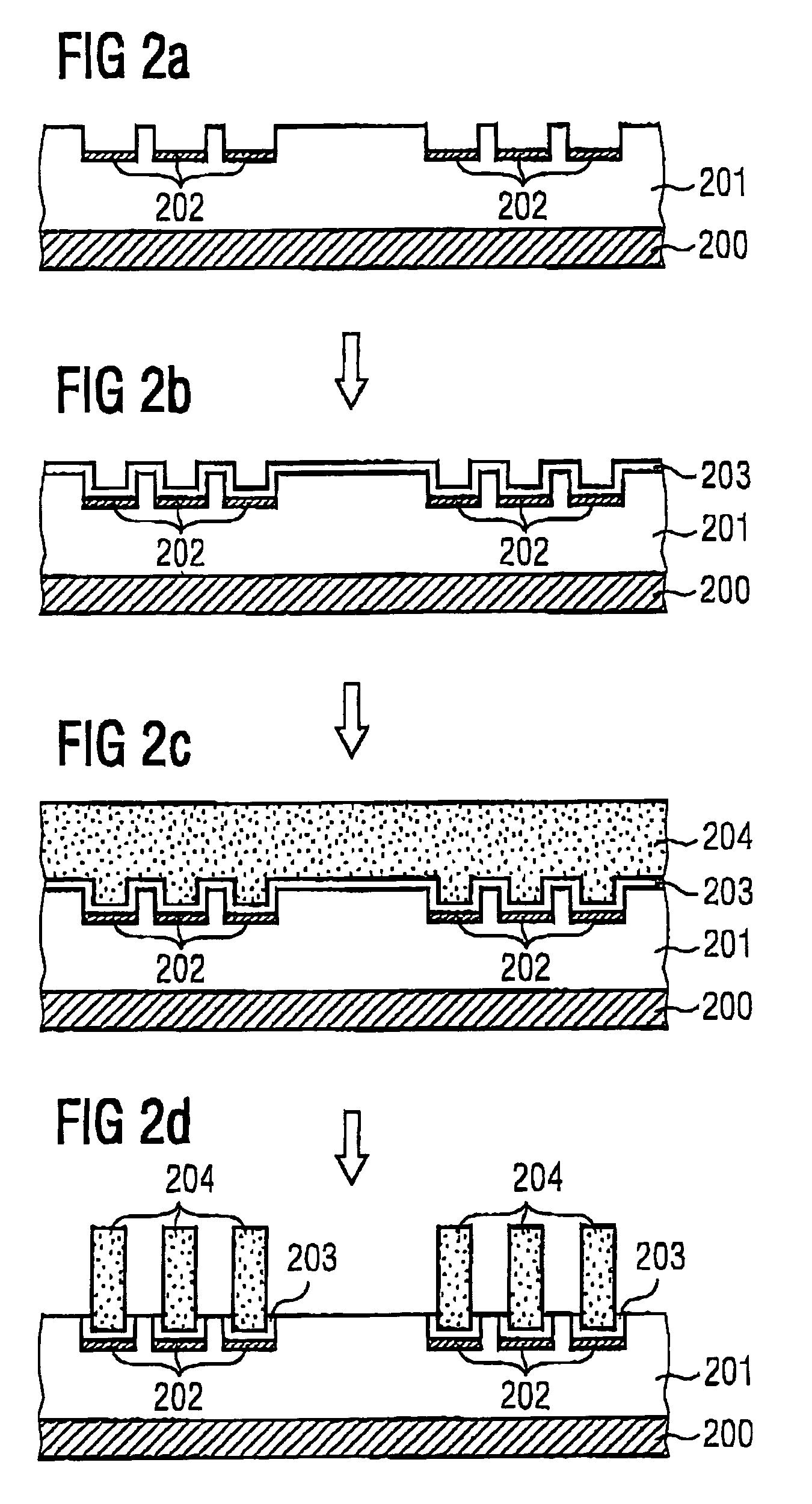
[0062]It should be noted that the illustration represented in FIG. 2c is a sectional view, i.e. the interconnects 202 extend both out from the area of the paper and in from the rear area of the paper, with the result that the regions uncovered by the removal of the passivation layer 201 are elongate, trench-shaped cutouts in the surface of the passivation layer 201. For this reason, the auxiliary layer 203 clinging tightly to these cutouts also assumes this elongate, trench-shaped configuration.

[0063]FIG. 2c shows the result of the application of a metal layer 204 on the auxiliary layer 203.

[0064]FIG. 2d shows the result of the removal of the metal layer 204 and of the auxiliary layer 203 in such a way that only those regions of the passivation layer 201 of the auxiliary layer 203 and of the metal layer 204 which are situated above the interconnects 202 of the coil remain after the removal process. Consequently, according to this exemplary embodiment, the metal layer 204 is separate...


PUM

PropertyMeasurementUnit
thicknessaaaaaaaaaa
thicknessaaaaaaaaaa
thicknessaaaaaaaaaa

Abstract

A method for fabricating a microelectronic circuit having an improved electrically conductive element. The method includes providing a finished processed microelectronic circuit having a monolithically integrated coil and having a passivation layer situated above at least the monolithically integrated coil. The method further comprises removing at least part of the passivation layer above the monolithically integrated coil and applying a metal layer above the monolithically integrated coil so that the metal layer is electrically coupled to the monolithically integrated coil.

Description

[0001]This application is a 371 of PCT / DE01 / 03792 Oct. 4, 2001.BACKGROUND OF THE INVENTION[0002]1. Field of the Invention[0003]A microelectronic circuit is disclosed in [1]. This microelectronic circuit is an integrated semiconductor element having an electrically conductive element (an inductor coil).[0004]2. Description of the Related Prior Art[0005]One problem with such electrically conductive elements known from the prior art is that their inherent conductivity is relatively low. This requires special operating conditions, such as e.g. low temperatures, or, under defined operating conditions, e.g. at defined temperatures, leads to a poor quality factor of the electrically conductive element. This in turn leads to a poor quality factor of the integrated semiconductor element having the conductive element.[0006]Furthermore, [2] describes a coil applied on a ceramic substrate.[0007][3] describes a method for repairing a semiconductor memory. In a semiconductor chip having fuses and...

Claims


Application Information

Patent Timeline
Patent Type & Authority Patents(United States)
IPC IPC(8): H01L21/20H01L21/4763H01F41/04H01L21/02H01L21/822H01L27/04H01L27/08
CPCH01L28/10H01L27/08H01L27/02
Inventor LAUTERBACH, CHRISTLPAULUS, CHRISTIAN
Owner INFINEON TECH AG
Why Eureka
Try Eureka