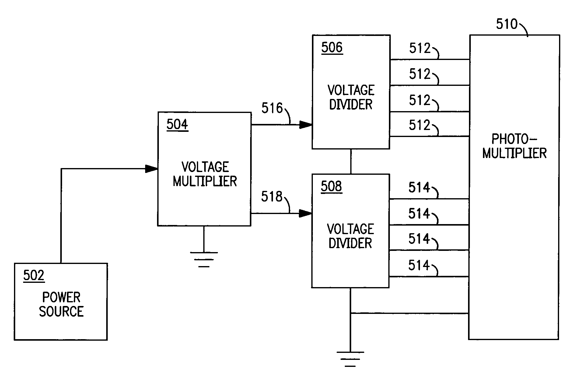
[0026]The present invention offers several photomultiplier tube voltage biasing circuits that provide more
latitude in tailoring the
voltage divider circuit for better optimization, and that will result in reduced
power consumption, wider linear operating ranges, and better stability. The improvements in performance are gained in two ways. First, it is recognized that the various intermediate voltage levels available from
voltage multiplier circuits can be used to improve the performance of the voltage divider network. Specifically, instead of using solely the maximum output voltage of the
voltage multiplier circuit and creating a succession of voltage levels from the maximum voltage using a voltage divider circuit, the intermediate voltage levels of the several stages of the voltage multiplier circuit are used to power subsections of the voltage divider network. This approach is based on the idea that the voltage divider network can be partitioned into several subsections to better optimize its performance, especially if these subsections of the voltage divider network can be separately and independently sourced by intermediate voltage output levels of a multistage voltage multiplier circuit.
[0027]For the case of partitioning the voltage divider circuit into two sections, there is then a ‘front-end’ section that generates voltage levels to bias the photomultiplier tube
photocathode and the dynodes near the photocathode, and a ‘back-end’ section of the voltage divider circuit that serves to bias the photomultiplier tube
anode and dynodes near the anode. The
electrode currents and loading of photocathode and dynodes biased by the front-end section are relatively low, and thus, a
resistor network is adequate to avoid saturation effects. The resistors comprising the voltage divider network for the front-end section can be of relatively
high resistance values in order to minimize the current drawn from the
high voltage multiplier.
[0029]The partitioning of the voltage divider circuit into sections and the use of intermediate voltage levels produced by stages of the voltage multiplier circuit to source sections of the voltage divider network, and thus permit their separate optimization, can considerably reduce the power drawn from the voltage multiplier. By partitioning the voltage divider network in two sections, the operating
power consumption can be reduced by almost a factor of two.
[0030]This separate optimization of the front-end and back-end sections of the voltage divider networks is facilitated by using intermediate voltage outputs from the several stages of the voltage multiplier circuit. The main benefit of such an optimization is to reduce the total power drawn from the high-voltage power supply and improve the stability and operating range of the photomultiplier tube. To
gain further reductions in power consumption, this approach can be extended, and the voltage divider circuit can be partitioned into three or more sections, each section sourced by an intermediate voltage level from the voltage multiplier circuit.
[0031]The backend section of the voltage divider circuit performs better when
transistor loads are used. A
transistor load, connected in an emitter follower configuration counters changes in load voltage with load current. Thus, the onset of saturation effects can be delayed as the radiation intensity increases. The optimization of series-connected transistors as a backend voltage divider network is also facilitated by the ability to source sections of the voltage divider network with intermediate voltage levels provided by the various stages of the voltage multiplier circuit.
[0032]Another aspect of the voltage divider that uses
transistor loads as described above is improved upon by the present invention. In particular, a ladder of series-connected transistors are clamped by a
current source such that the emitter current is approximately constant, independent of the
electrode load. The
current source fixes the biases across
electrode pairs that is, to a good approximation, independent of the voltage used to source the string of transistors. Thus, the optimum transistors can be set relatively independent of the
high voltage source and as a consequence, no
safety margin needs to be designed into the voltage divider circuit for operating at reduced source voltage levels. By eliminating the need to overrate the voltage divider circuit currents, a three- to four-fold reduction in power consumption can be gained.

