Process for manufacturing a printed wiring board

a manufacturing process and wiring board technology, applied in the direction of resistive material coating, metallic pattern coating, metallic material coating process, etc., can solve the problems of not being able to meet the needs of commoning bars for electrical connections, wasting valuable space that could otherwise be used for placement of additional circuitry or other features, and simply being unable to meet the needs of commoning bars, etc., to achieve high conductive

a manufacturing process and wiring board technology, applied in the direction of resistive material coating, metallic pattern coating, metallic material coating process, etc., can solve the problems of not being able to meet the needs of commoning bars for electrical connections, wasting valuable space that could otherwise be used for placement of additional circuitry or other features, and simply being unable to meet the needs of commoning bars, etc., to achieve high conductive

US7007378B2Inactive Publication Date: 2006-03-07GLOBALFOUNDRIES INC

Image

  • Process for manufacturing a printed wiring board
  • Process for manufacturing a printed wiring board

Examples


Embodiment Construction

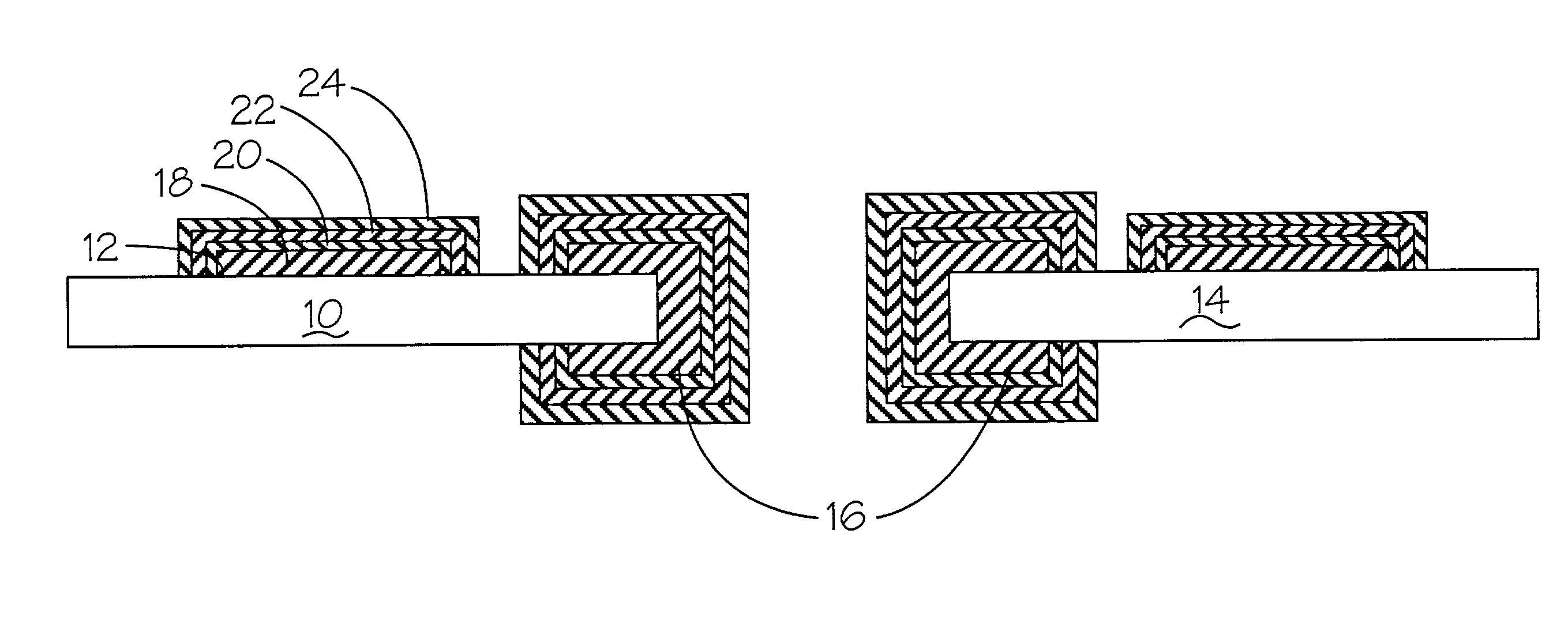
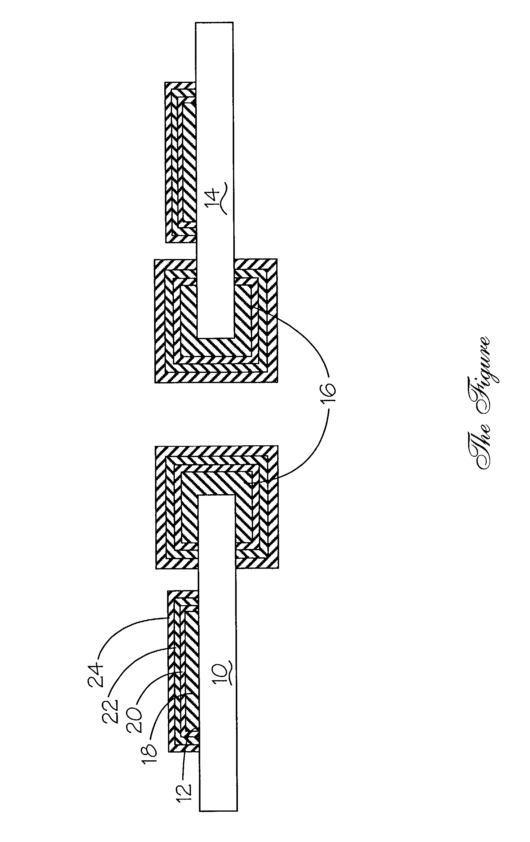
[0026]The present invention provides a printed wiring board that has incorporated as part of its features a connection site or multiple connection sites to external components. Examples of types of connection sites that can be used in this invention are: land grid arrays, surface mount pads, and ball grid arrays. Land grid arrays comprise multiple plated pads to which the external component is attached.

[0027]Examples of such external components include integrated circuit chip carriers, modules, and the like. Physical connection can be made in various ways, including soldering, or by direct physical contact through connectors from the external components. Such external connectors typically have a mechanism ensuring contact by means that create a positive holding force to the connection site on the printed wiring board. The attachment and removal of these external components can cause abrasion, wear, and deformation of the connection sites, especially when these external components ar...


PUM

PropertyMeasurementUnit
thicknessaaaaaaaaaa
thicknessaaaaaaaaaa
thicknessaaaaaaaaaa

Abstract

A process for manufacturing a land grid array connector for a printed wiring board is disclosed. The process does not require electroplating precious metal overlays. Therefore, no commoning bar is required. Another benefit of the invention includes a connector design using only a flash, soft gold application in the outer surface of the connector. Physical hardness and durability are derived from a thin palladium layer lying beneath the flash gold layer.

Description

RELATED PATENT APPLICATION[0001]The present patent application is a continuation in-part to U.S. patent application Ser. No. 09 / 344,322, filed on Jun. 24, 1999, now abandoned.FIELD OF THE INVENTION[0002]This invention relates to a high performance electronic connector, such as a land grid array, having very high density per unit of area, and to a method of fabrication and utilization of such a connector to achieve improved performance, quality, and reliability compared to prior arrangements.BACKGROUND OF THE INVENTION[0003]Electronic circuits and, more particularly, the more complex circuits found in computer logic systems, frequently employ one or more printed circuit or wiring boards on which various components or elements are mounted. To electronically interconnect these components to printed circuit boards for feeding electrical power and signals to the circuit elements, various connector arrangements are utilized. Examples of components of the external system are integrated cir...

Claims


Application Information

Patent Timeline
07 Mar 2006
Publication
US7007378B2
IPC
H01R9/00; H05K3/24
CPC
H05K3/244; Y10T29/49147; Y10T29/49117; Y10T29/49165; Y10T428/24917; Y10T29/49155
Inventors
GAUDIELLO, JOHN G.; HERARD, JAMES D.