Glass frit bond and process therefor

a technology of glass frit and bonding technology, applied in the field of glass frit compositions, can solve the problems of glass susceptible to moisture attack, inability to produce vacuum seals, and incompatible or less than ideal bonding techniques for certain applications

Inactive Publication Date: 2006-03-07
DELPHI TECH IP LTD
View PDF2 Cites 8 Cited by
  • Summary
  • Abstract
  • Description
  • Claims
  • Application Information

AI Technical Summary

Benefits of technology

[0014]Glass frit materials protected with a lead phosphate coating in accordance with this invention are particularly well suited for bonding device and capping chips together, such as where the glass frit material is used to hermetically seal a cavity defined by and between the device chip and the capping chip. In such an application, the lead phosphate coating prevents the lead content of the glass frit material from reacting with moisture, such that lead is not released to react with aluminum metallization on the chips and create holes that would degrade the hermetical seal formed by the glass frit material.

Problems solved by technology

As would be expected, each of these bonding techniques can be incompatible or less than ideal for certain applications.
Silicon direct and anodic bonding methods require very smooth bonding surfaces, and therefore cannot produce a vacuum seal when trench isolation or unplanarized metal crossunders are employed on the device wafer, such as to electrically interconnect a MEMS device to bond pads outside the vacuum-sealed cavity of the package.
However, the percentage of lead required in a glass frit material to achieve high quality wafer-level sealing at low firing temperatures makes the resulting glass susceptible to attack by moisture.
When a lead-containing glass is exposed to moisture, lead can be released from the glass and, in concert with moisture, migrate to exposed aluminum metallization on the wafer, resulting in galvanic corrosion of the metallization.
This corrosion is a source of concern for both the wafer-level yield and the system-level reliability of a semiconductor device.
Glass frit used in wafer bonding processes is often exposed to attack by moisture as a result of the use of water to cool the wafers and remove debris during the dicing operation used to singulate dies from the wafers.
During singulation, the glass bond line is generally covered by water for the duration of the dicing operation, making the glass-water interaction difficult to avoid.
Following dicing, if the device is placed in a package that is not hermetically sealed, the glass bond line may be subjected to prolonged exposure to moisture during the operating life of the device.

Method used


Image

  • Glass frit bond and process therefor
  • Glass frit bond and process therefor

Examples


Embodiment Construction

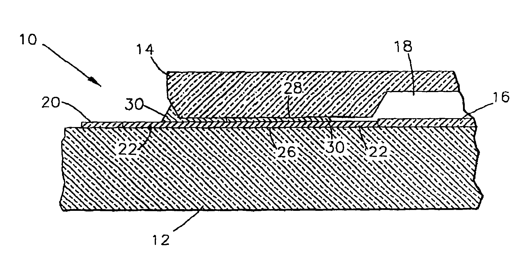
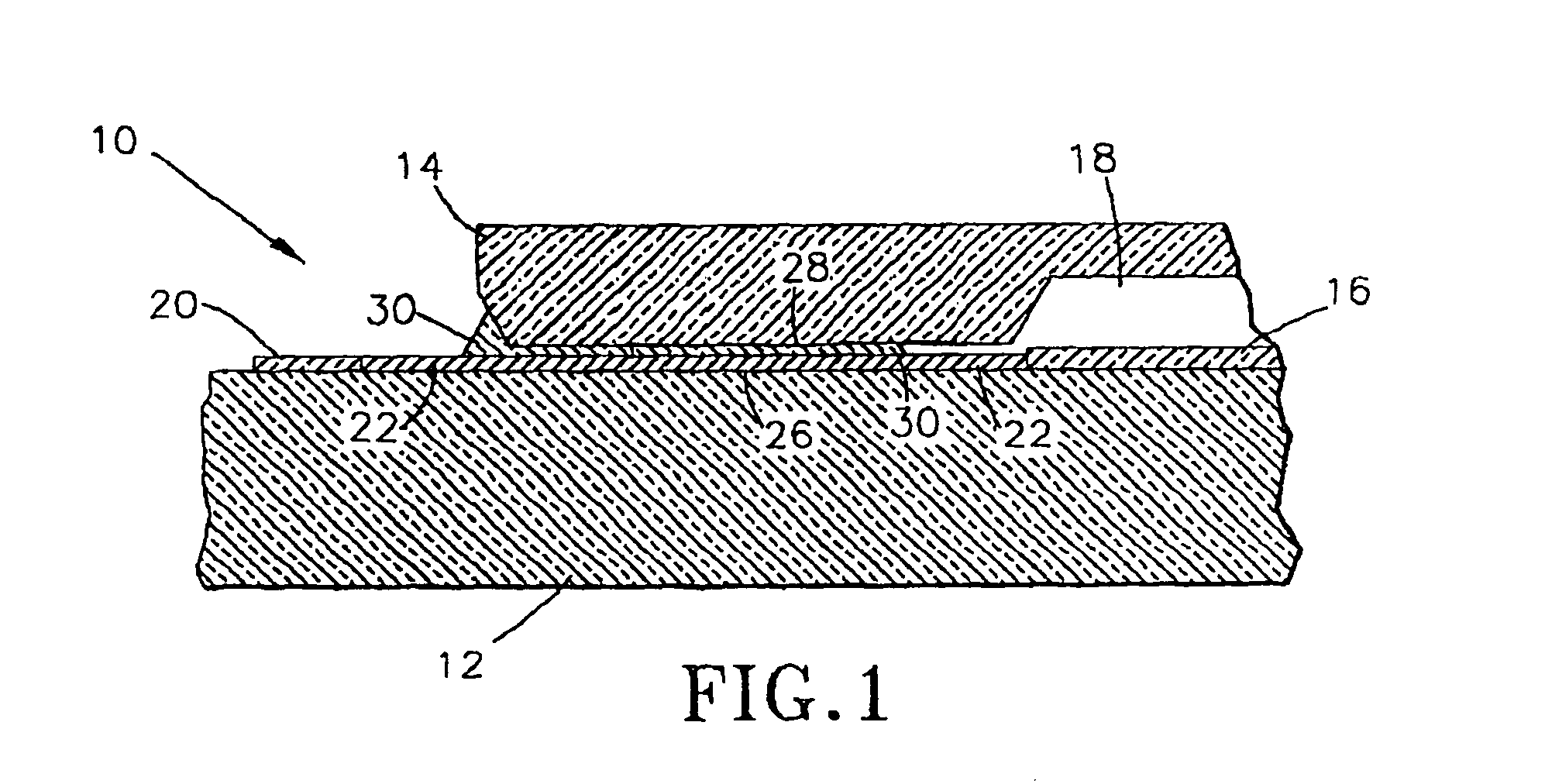
[0017]FIG. 1 represents a portion of a MEMS device package 10 formed by glass frit bonding a device wafer 12 to a capping wafer 14, such that a micromachined structure 16 (schematically represented in FIG. 2) is enclosed within a cavity 18 between the wafers 12 and 14. The device wafer 12 is typically formed of a semiconductor material such as silicon, preferably monocrystallographic silicon, though it is foreseeable that other materials could be used. The capping wafer 14 may be formed of glass, ceramic, or a semiconducting material. The micromachined structure 16 can be of any desired type, such as a proof mass, resonating structure, diaphragm or cantilever that relies on capacitive, piezoresistive and piezoelectric sensing elements to sense acceleration, motion, pressure, etc., all of which are known in the art.

[0018]As is conventional, the micromachined structure 16 is electrically interconnected to metal bond pads 20 on the device wafer 12 by conductive runners 22, often in the...


PUM

PropertyMeasurementUnit
softening pointaaaaaaaaaa
temperatureaaaaaaaaaa
volumeaaaaaaaaaa

Abstract

A lead-containing glass material of the type suitable for use in a wafer bonding process, wherein the moisture resistance of the glass material is increased by the presence of a lead phosphate coating on an outer exposed surface of the material, thereby acting as a barrier to reaction of moisture with the lead of the glass material. A source of reactive phosphate ions is applied to the glass material so as to spontaneously form the desired lead phosphate coating.

Description

CROSS REFERENCE TO RELATED APPLICATIONS[0001]This application is a Div of Ser. No. 10 / 248,503 Jan. 24, 2003 U.S. Pat. No. 6,815,071.STATEMENT REGARDING FEDERALLY SPONSORED RESEARCH[0002]Not applicable.BACKGROUND OF THE INVENTION[0003](1) Field of the Invention[0004]The present invention generally relates to glass frit compositions. More particularly, this invention relates to lead-containing glass frit materials of the type suitable for use in wafer bonding processes, wherein the moisture resistance of the glass frit material after firing is increased by a lead phosphate coating formed on an exposed outer surface of the glass frit material.[0005](2) Description of the Related Art[0006]Within the semiconductor industry, there are numerous applications that require bonding a semiconductor wafer to a second wafer or glass substrate. As an example, a microelectromechanical system (MEMS) device formed in or on a semiconductor wafer (referred to herein as a device wafer) is often capped b...

Claims


Application Information

Patent Timeline
Patent Type & Authority Patents(United States)
IPC IPC(8): H01L21/46C03C8/08C03C8/10C03C17/02C03C17/04C04B37/02
CPCB81C1/00269C03C8/08C03C17/02C03C17/04C04B37/025C03C8/10B81C2203/0109B81C2203/019C04B2237/30C04B2237/10
Inventor BANEY, WILLIAM J.BANEY, BRENDA B.HUDE, HEATHER
Owner DELPHI TECH IP LTD
Why Eureka
Try Eureka