Out of the box vertical transistor for eDRAM on SOI

a vertical transistor and soi substrate technology, applied in the field of vertical memory devices, can solve the problems of affecting the electrical communication of the memory device, the thickness of the upper silicon containing layer of the soi substrate, 100 nm, and being too thin to accompany the formation of the entire vertical devi

Active Publication Date: 2006-03-07
GLOBALFOUNDRIES US INC
View PDF3 Cites 22 Cited by
  • Summary
  • Abstract
  • Description
  • Claims
  • Application Information

AI Technical Summary

Problems solved by technology

In prior devices, if the vertical device is positioned below the buried insulating layer, the buried insulating layer produces a vertical discontinuity, where electrical communication to the memory device is negatively impacted.
Additionally, the thickness of the upper silicon containing layer of the SOI substrate, typically being on the order of about 70 nm to about 100 nm, is too thin to accompany the formation of the entire vertical device without extending into the underlying buried insulating layer.

Method used


Image

  • Out of the box vertical transistor for eDRAM on SOI
  • Out of the box vertical transistor for eDRAM on SOI
  • Out of the box vertical transistor for eDRAM on SOI

Examples


Embodiment Construction

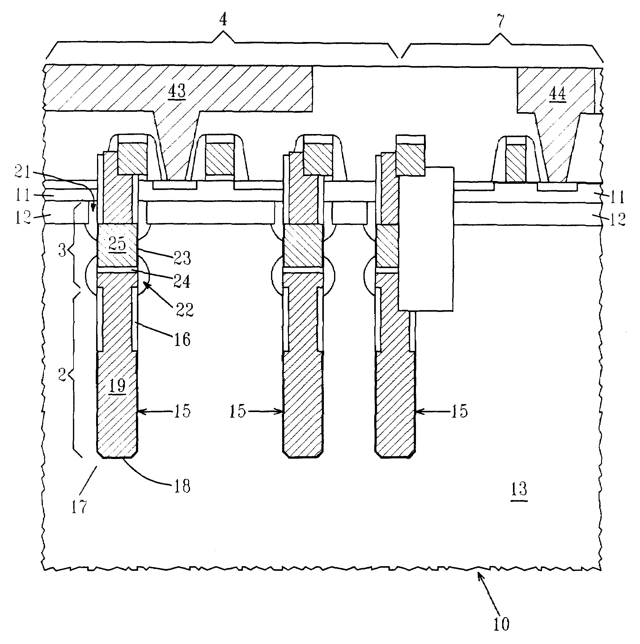
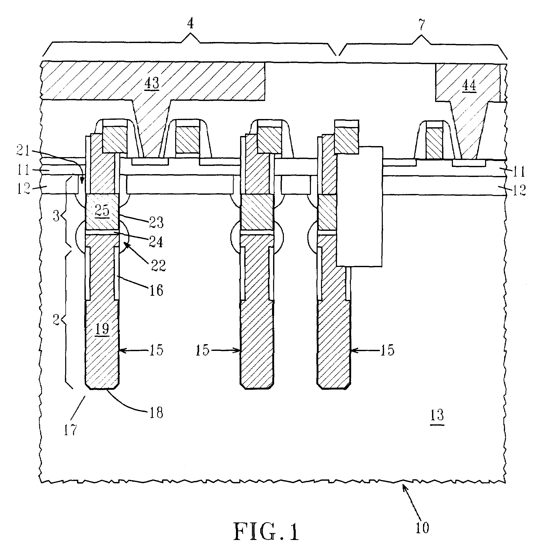
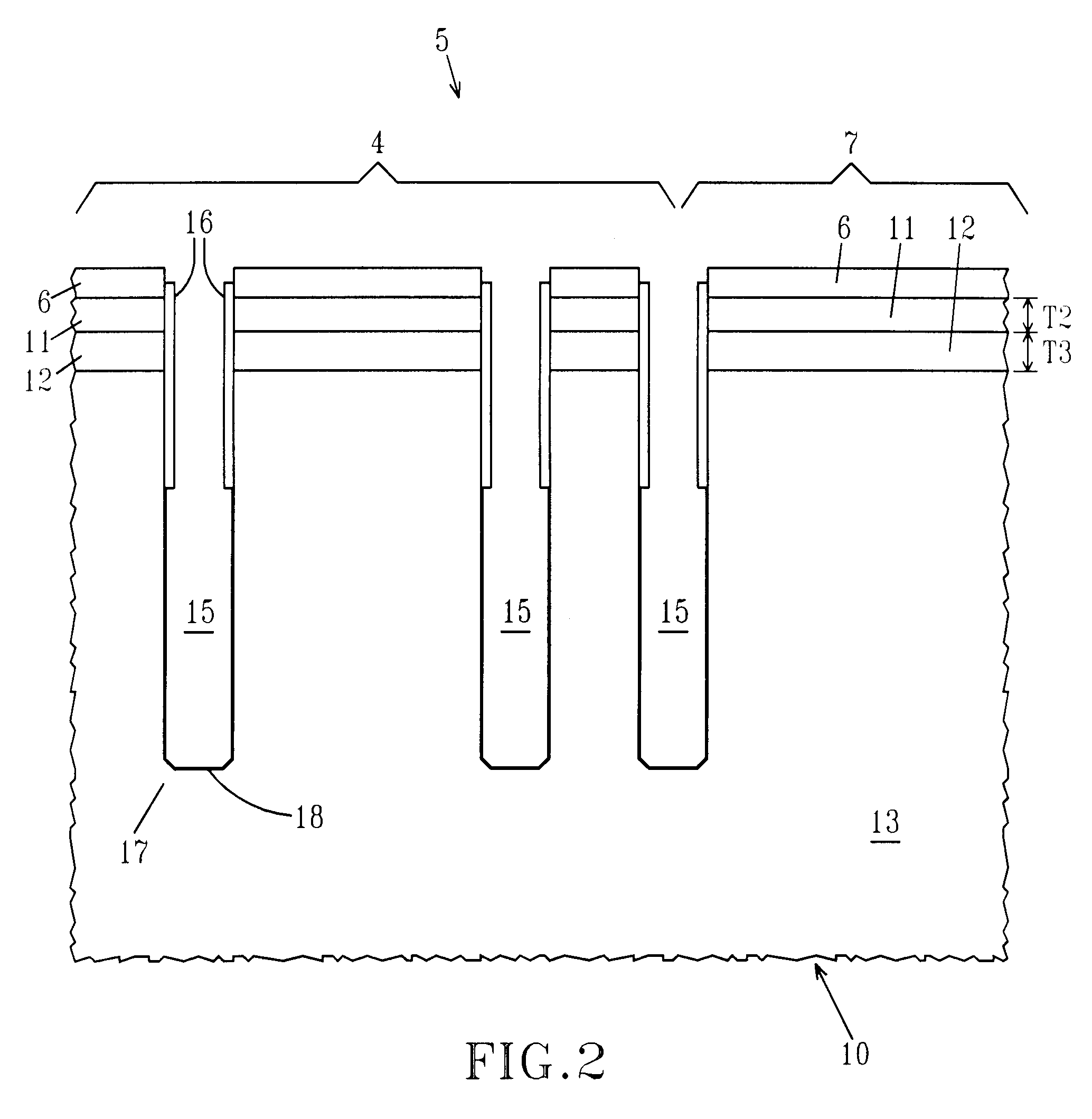
[0020]A memory array and support structure in SOI substrates, and method of forming the same, will now be discussed in greater detail by referring to the drawings that accompany the present application. In the accompanying drawings, like and corresponding parts are referred to by like reference numbers. Although the drawings show the presence of an array region containing only two memory devices and a support region containing only a single logic device, multiple memory devices and multiple logic devices are also within the scope of the present invention.

[0021]The present memory array and support structure combines the high-drive current and high-density characteristics possible in a vertical memory device, with the superior logic devices formed on a silicon-on-insulators (SOI) substrate. The advantages of forming logic devices on SOI substrates include higher packing density, the reduction of latch-up effects, lower junction capacitance, suitability to low-voltage applications, and...


PUM


Abstract

The present invention provides a vertical memory device formed in a silicon-on-insulator substrate, where a bitline contacting the upper surface of the silicon-on-insulator substrate is electrically connected to the vertical memory device through an upper strap diffusion region formed through a buried oxide layer. The upper strap diffusion region is formed by laterally etching a portion of the buried oxide region to produce a divot, in which doped polysilicon is deposited. The upper strap region diffusion region also provides the source for the vertical transistor of the vertical memory device. The vertical memory device may also be integrated with a support region having logic devices formed atop the silicon-on-insulator substrate.

Description

BACKGROUND OF INVENTION[0001]The present invention relates to electronic devices, and more particularly to vertical memory devices, such as eDRAM devices, formed within a silicon-on-insulator (SOI) substrate.[0002]Dynamic Random Access Memory (DRAM) cells are well known. A DRAM cell is essentially a capacitor for storing charge and a pass transistor (also called a pass gate or access transistor) for transferring charge to and from the capacitor. Data (1 bit) stored in the cell is determined by the absence or presence of charge on the storage capacitor. Because cell size affects chip density, and cost, reducing cell area is one of the DRAM designer's primary goals.[0003]One way to accomplish this density goal without sacrificing storage capacitance is to use trench capacitors in the cells. Trench capacitors can be formed by etching deep trenches in a silicon wafer and forming vertically orientated capacitors within each deep trench. Thus, the surface area required for the storage cap...

Claims


Application Information

Patent Timeline
Patent Type & Authority Patents(United States)
IPC IPC(8): H01L27/108H01L21/8242H01L31/119
CPCH01L27/10841H01L27/10864H01L27/10867H10B12/395H10B12/0383H10B12/0385
Inventor ADKISSON, JAMES W.BRONNER, GARY B.CHIDAMBARRAO, DURESETIDIVAKARUNI, RAMACHANDRARADENS, CARL J.
Owner GLOBALFOUNDRIES US INC
Why Eureka
Try Eureka