Semiconductor memory device having easily redesigned memory capacity

a memory device and memory technology, applied in the direction of information storage, static storage, digital storage, etc., can solve the problem of more complicated change to the refresh address counter, and achieve the effect of convenient redesigned memory capacity

Inactive Publication Date: 2006-03-07
RENESAS TECH CORP
View PDF5 Cites 0 Cited by
  • Summary
  • Abstract
  • Description
  • Claims
  • Application Information

AI Technical Summary

Benefits of technology

[0009]An object of the present invention is to provide a semiconductor memory device having a configuration to allow a memory capacity to be easily redesigned.
[0012]In accordance with the present invention, therefore, there can be provided a semiconductor memory device where a memory capacity can easily be redesigned and the number of bits of a refresh counter can be reduced with a reduced circuit area.

Problems solved by technology

Furthermore, a more complicated change has to be made to the refresh address counter to support the memory capacity where the number of sub-blocks and the total number of word lines is not the power of two.

Method used


Image

  • Semiconductor memory device having easily redesigned memory capacity
  • Semiconductor memory device having easily redesigned memory capacity
  • Semiconductor memory device having easily redesigned memory capacity

Examples


first embodiment

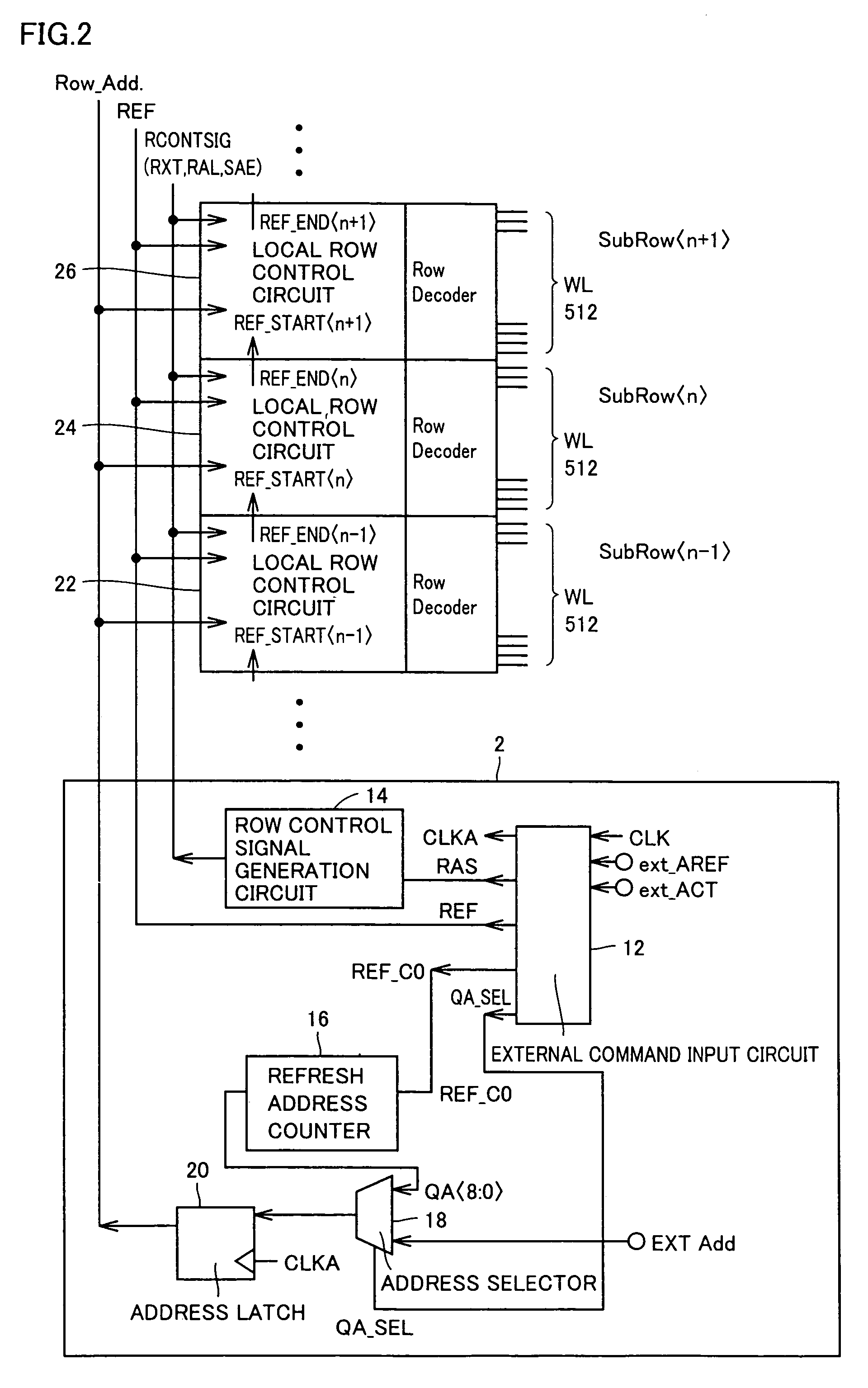
[0034][First Embodiment]

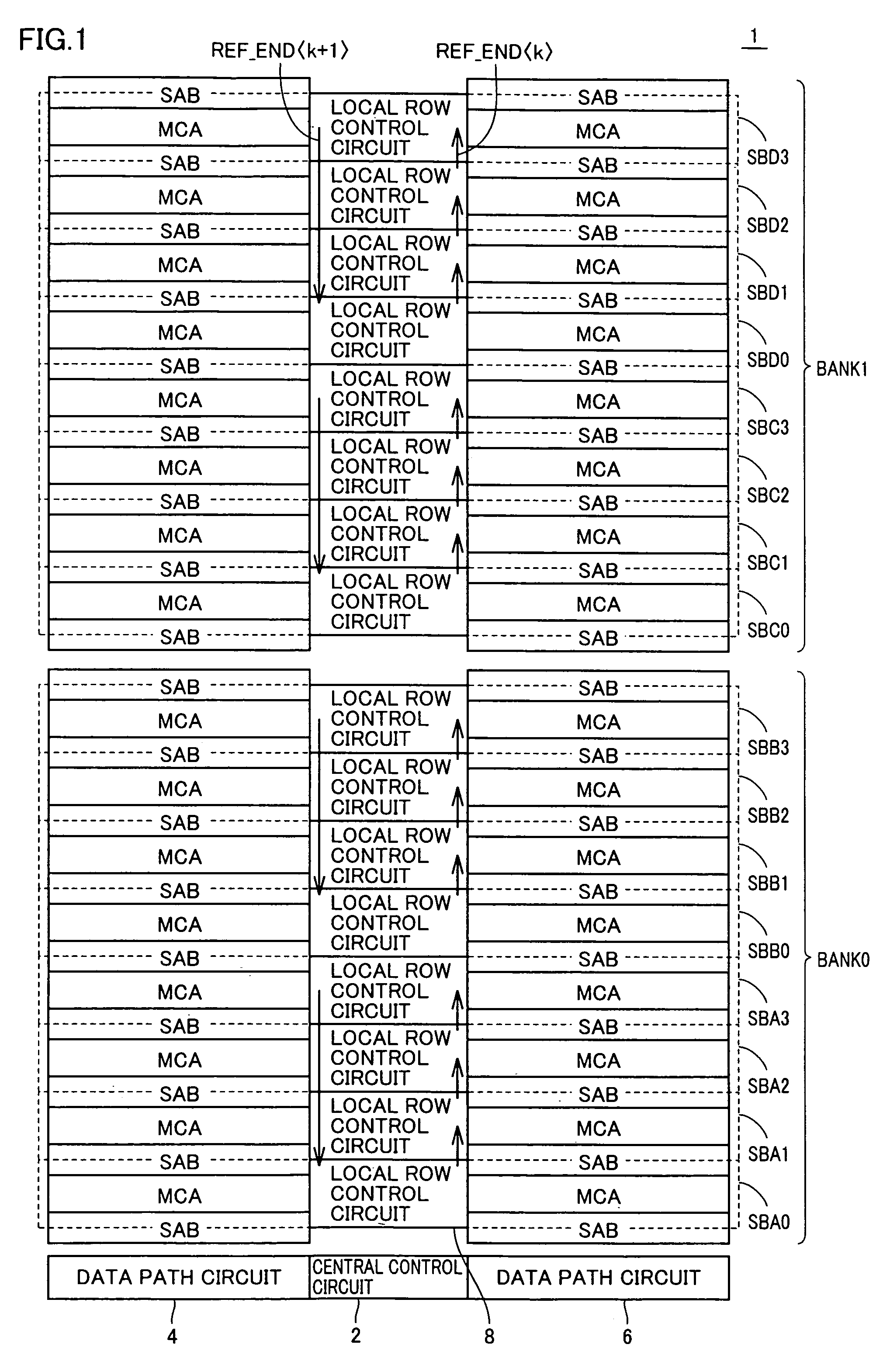
[0035]FIG. 1 is a block diagram showing a configuration of a semiconductor memory device in accordance with an embodiment of the present invention.

[0036]Referring to FIG. 1, an embedded memory core 1 configured with two banks will be described. Memory core 1 includes a central control circuit 2, data path circuits 4, 6, and memory banks BANK0, BANK1. Each of data path circuits 4, 6 is a circuit performing data control in reading and writing.

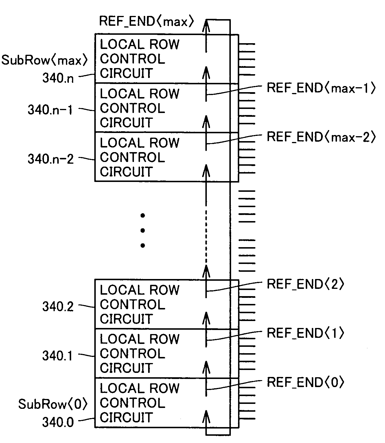
[0037]Each memory bank includes eight sub-blocks. Specifically, bank BANK0 includes sub–blocks SBA0–SBA3, SBB0–SBB3. Memory bank BANK1 includes sub-blocks SBC0–SBC3, SBD0–SBD3. Sub-blocks SBA0–SBA3 are arranged in order. Sub-blocks SBB0–SBB3 are arranged in order. Sub-blocks SBD0–SBD3 are arranged in order.

[0038]Each sub-block includes one local row control circuit 8 and two memory cell arrays MCA arranged on opposite sides thereof. A sense amplifier band SAB is arranged between a memory cell array MCA and a memory cell ar...

second embodiment

[0135][Second Embodiment]

[0136]As described with reference to FIG. 13, the refresh end signal is successively shifted to a sub-block to be next refreshed. A loop of a signal transmitting path is formed such that the refresh end signal of the last sub-block is input to the first sub-block. The refresh cycle may easily be changed by only changing the number of sub-blocks included in this loop.

[0137]FIG. 14 is a diagram illustrating a loop realizing 1.5K refresh cycle.

[0138]Referring to FIG. 14, local row control circuits 341–346 are provided in respective different sub-blocks. Each sub-block includes 512 word lines. Three local row control circuits 341–343 form a loop in which a refresh end signal is circulated. Three local row control circuits 344–346 form a loop in which a refresh end signal is circulated.

[0139]The semiconductor memory device employing the present invention can easily realize the refresh cycle that is not the power of two, which is difficult to realize with a circui...

third embodiment

[0147][Third Embodiment]

[0148]In addition to the description in the first and second embodiments, partial refresh can be realized by stopping a refresh start signal in a particular sub-block group of a plurality of sub-block groups in which a refresh end signal loops.

[0149]FIG. 18 is a diagram conceptually illustrating a partial refresh control.

[0150]Referring to FIG. 18, in local row control circuits 361–364, a refresh end signal is successively transmitted for continuous refresh operation. On the other hand, in local row control circuits 365–368, refresh is performed in a circulating manner when refresh stop signal STOP_REF is inactivated. When refresh stop signal STOP_REF is activated, however, local row control circuit 365 does not transmit the refresh end signal to the next stage so that the refresh operation can be stopped. The partial refresh can be realized by providing such a gate circuit 369 in one local row control circuit 365 in a loop that transmits the refresh end sign...


PUM


Abstract

Sub-blocks SBA0–SBA3, SBB0–SBB3, SBC0–SBC3, SBD0–SBD3 respectively form four groups. In each group, a refresh end signal REF_END is successively transferred to the next sub-block. Therefore, when a refresh counter of the number of bits corresponding to the number of word lines present in a sub-block is provided in a central control circuit, a memory capacity can easily be redesigned by changing the number of sub-blocks and changing a group configuration of sub-blocks. As a result, there can be provided a memory core for embedded memory in which a memory capacity can easily be changed and a refresh control-related circuitry can easily be changed.

Description

BACKGROUND OF THE INVENTION[0001]1. Field of the Invention[0002]The present invention relates to a semiconductor memory device, and more particularly to a refresh control circuit used for embedded DRAM (Dynamic Random Access Memory) or the like.[0003]2. Description of the Background Art[0004]In DRAM, refresh operations are essential to retain stored data. Japanese Patent Laying-Open No. 3-80493 discloses a memory refresh circuit. This document describes that a refresh end signal of each memory bank serves as a refresh request signal for a bank control circuit at the next stage and the refresh end signal of the memory bank at the last stage is supplied to a refresh request circuit as an acknowledge signal.[0005]In this manner, the refresh operations of the memory banks do not overlap, thereby effectively preventing an error in the system having the memory banks.[0006]Recently, embedded memory has been developed where DRAM and the other large-scale logic circuit or a microprocessor ar...

Claims


Application Information

Patent Timeline
Patent Type & Authority Patents(United States)
IPC IPC(8): G11C8/00G11C11/406G11C8/12G11C11/401
CPCG11C8/12
Inventor WATANABE, NAOYA
Owner RENESAS TECH CORP
Why Eureka
Try Eureka