Method of forming a photosensitive pattern, method of manufacturing a display substrate, and display substrate

a technology of display substrate and photosensitive pattern, which is applied in the direction of photomechanical equipment, printing, instruments, etc., can solve the problems of significantly increasing the production cost of display devices, significantly increasing the manufacturing cost of display substrates, and significantly reducing so as to improve the reliability of manufacturing thin-film patterns and the effect of reducing production costs

Active Publication Date: 2014-09-30
SAMSUNG DISPLAY CO LTD
View PDF4 Cites 0 Cited by
  • Summary
  • Abstract
  • Description
  • Claims
  • Application Information

AI Technical Summary

Benefits of technology

[0008]One or more embodiments of the present invention provide a method of forming a photosensitive pattern capable of improving the reliability of a manufacturing process.
[0024]Therefore, although manufacturing conditions are changed, the operator may predict actually exposed positions so that the thin-film pattern may be easily redesigned to improve a reliability of manufacturing the thin-film pattern. In addition, the reliability of a display substrate including the thin-film pattern or formed using the thin-film pattern and the reliability of manufacturing the display substrate may be improved.

Problems solved by technology

Since the cost of manufacturing the mask is significantly high, the mask used for the photolithography process substantially increases the manufacturing cost of display substrates, and therefore substantially increases the production cost of display devices.
Because of the difference between the theoretically calculated irradiated position and the actual irradiated position, a predetermined position preset by an operator may not receive a light with sufficient light intensity, and thus a photoresist pattern formed using the digital exposure device has portions in which the light is not desirably provided.
As a result, the reliability of the photoresist pattern and the pattern formed using the photoresist pattern may be undesirable.

Method used


Image

  • Method of forming a photosensitive pattern, method of manufacturing a display substrate, and display substrate
  • Method of forming a photosensitive pattern, method of manufacturing a display substrate, and display substrate
  • Method of forming a photosensitive pattern, method of manufacturing a display substrate, and display substrate

Examples


Embodiment Construction

[0041]Hereinafter, the present invention will be explained in detail with reference to the accompanying drawings.

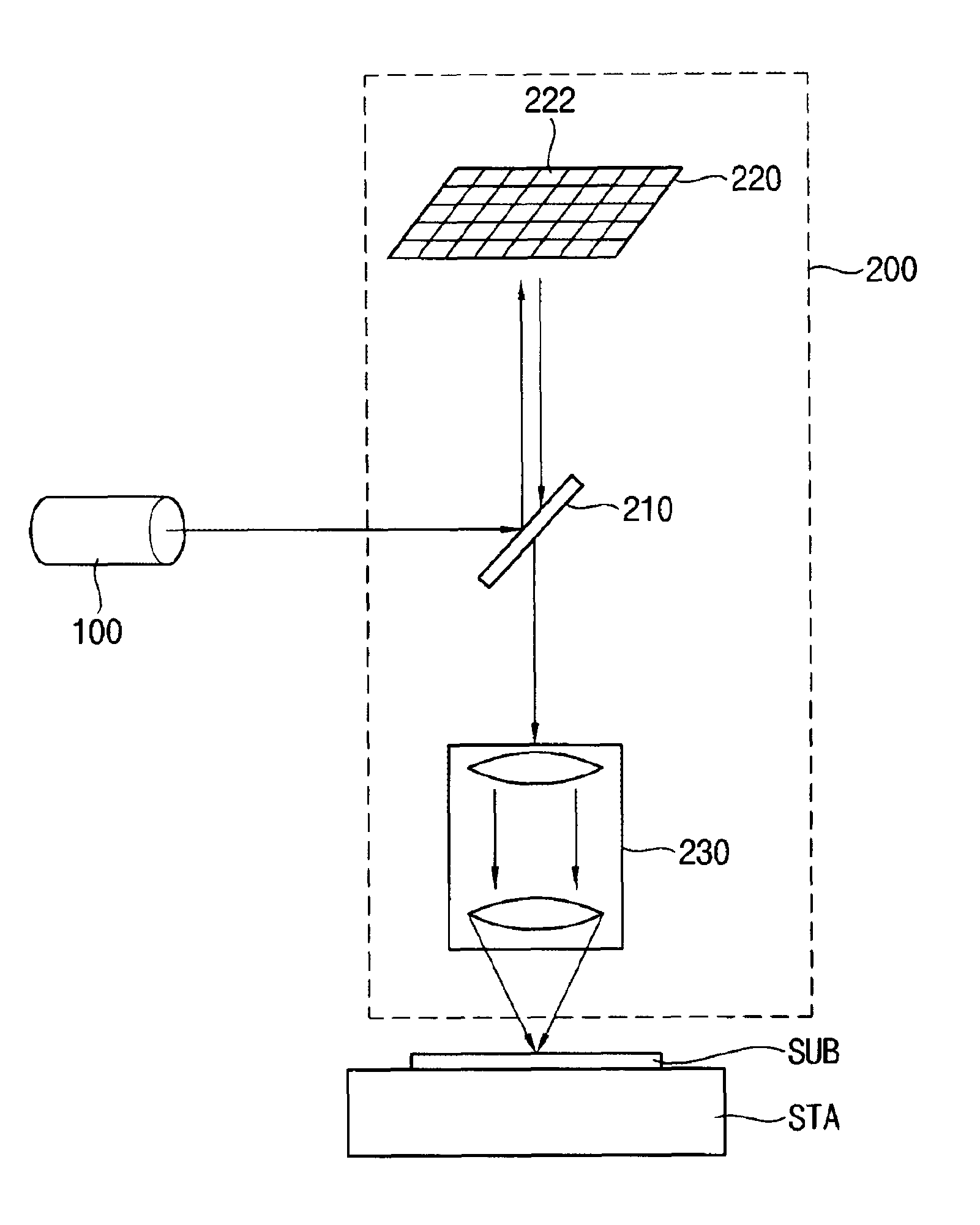
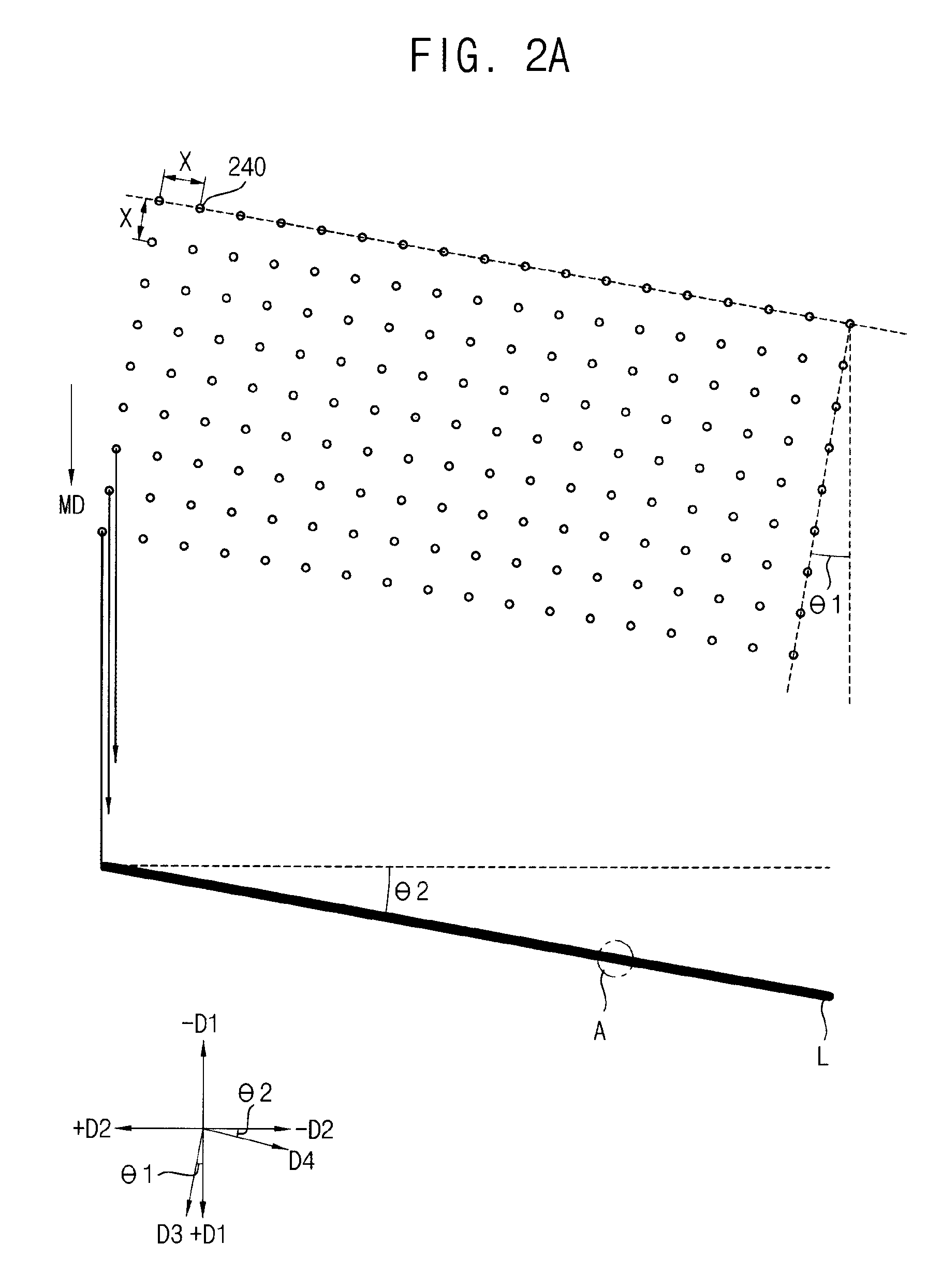
[0042]FIG. 1 is a conceptual view illustrating a digital exposure device for forming a photosensitive pattern according to one or more embodiments of the present invention. FIG. 2A is a plan view illustrating an exposure step performed on a photosensitive layer using an optical head in FIG. 1, and FIG. 2B is an enlarged view of a portion ‘A’ in FIG. 2A.

[0043]As illustrated in the example of FIG. 1, the digital exposure device includes a light source 100 generating a light, an optical head 200 receiving the light from the light source 100, and a stage STA receiving the light from the optical head 200. Operation of the digital exposure device is now discussed.

[0044]The light source 100 emits a laser beam to the optical head 200.

[0045]The optical head 200 includes a beam splitter 210, a digital micro-mirror device (“DMD”) 220, and an optical system 230.

[0046]The beam splitte...


PUM

PropertyMeasurementUnit
acute angleaaaaaaaaaa
angleaaaaaaaaaa
angleaaaaaaaaaa

Abstract

A method of forming a photosensitive pattern on a substrate with a photosensitive layer disposed thereon may include moving at least one of the substrate and a set of micro-mirrors in a first direction, the set of micro-mirrors being disposed above the substrate and being arranged as an array, the array having a first edge extending in a second direction, the second direction being at an acute angle with respect to the first direction. The method may also include selectively turning on one or more micro-mirrors of the set of micro-mirrors according to a position of the set of micro-mirrors relative to the photosensitive layer, thereby irradiating one or more spot beams on the photosensitive layer. The photosensitive layer exposed by the spot beams is developed to form a photosensitive pattern having an edge portion extending in a third direction crossing the first and second directions.

Description

CROSS-REFERENCE TO RELATED APPLICATIONS[0001]This application claims priority under 35 U.S.C. §119 to Korean Patent Application No. 2011-25494, filed on Mar. 22, 2011 in the Korean Intellectual Property Office (KIPO), the contents of which are herein incorporated by reference in its entirety.BACKGROUND OF THE INVENTION[0002]1. Field of the Invention[0003]Example embodiments of the present invention relate to a method of forming a photosensitive pattern, a method of manufacturing a display substrate, and a display substrate. More particularly, example embodiments of the present invention relate to a method of forming a photosensitive pattern using a digital exposure device (which includes micro-mirrors), a method of manufacturing a display substrate using the digital exposure device, and a display substrate.[0004]2. Description of the Related Art[0005]Generally, a thin-film transistor (“TFT”) and signal lines electrically connected to the TFT are formed by a photolithography process....

Claims


Application Information

Patent Timeline
Patent Type & Authority Patents(United States)
IPC IPC(8): H01L29/04G03F7/20H01L27/12
CPCG03F7/70291G03F7/70508H01L27/1288
Inventor PARK, JUNG-INSIM, SU-YEONYUN, SANG-HYUNKIM, CHA-DONGLEE, HI-KUK
Owner SAMSUNG DISPLAY CO LTD
Why Eureka
Try Eureka