
Microcomputer

a microcomputer and microprocessor technology, applied in the field of microcomputers, can solve the problems of inability to advance the automatic layout generator of an analog circuit, leakage current, and increased power consumption in the sleep mode, so as to achieve the effect of reducing the power consumption of backing up data during the sleep mode, facilitating redesign, and easy redesign

Inactive Publication Date: 2009-01-27
DENSO CORP
View PDF9 Cites 1 Cited by
  • Summary
  • Abstract
  • Description
  • Claims
  • Application Information

AI Technical Summary

Benefits of technology

Reduces power consumption during sleep mode by minimizing leak current and allows for easy redesign of the microcomputer when manufacturing processes change, maintaining efficient operation across different process nodes.

Problems solved by technology

Therefore, a leak current occurs regardless of whether the logic circuits operate and the power consumption in the sleep mode is increased.
However, an automatic layout generator for an analog circuit has not been advanced yet.

Method used


Image

  • Microcomputer
  • Microcomputer
  • Microcomputer

Examples


Embodiment Construction

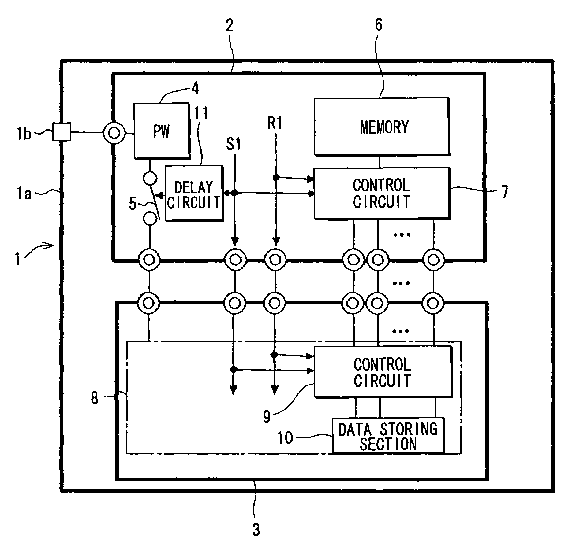
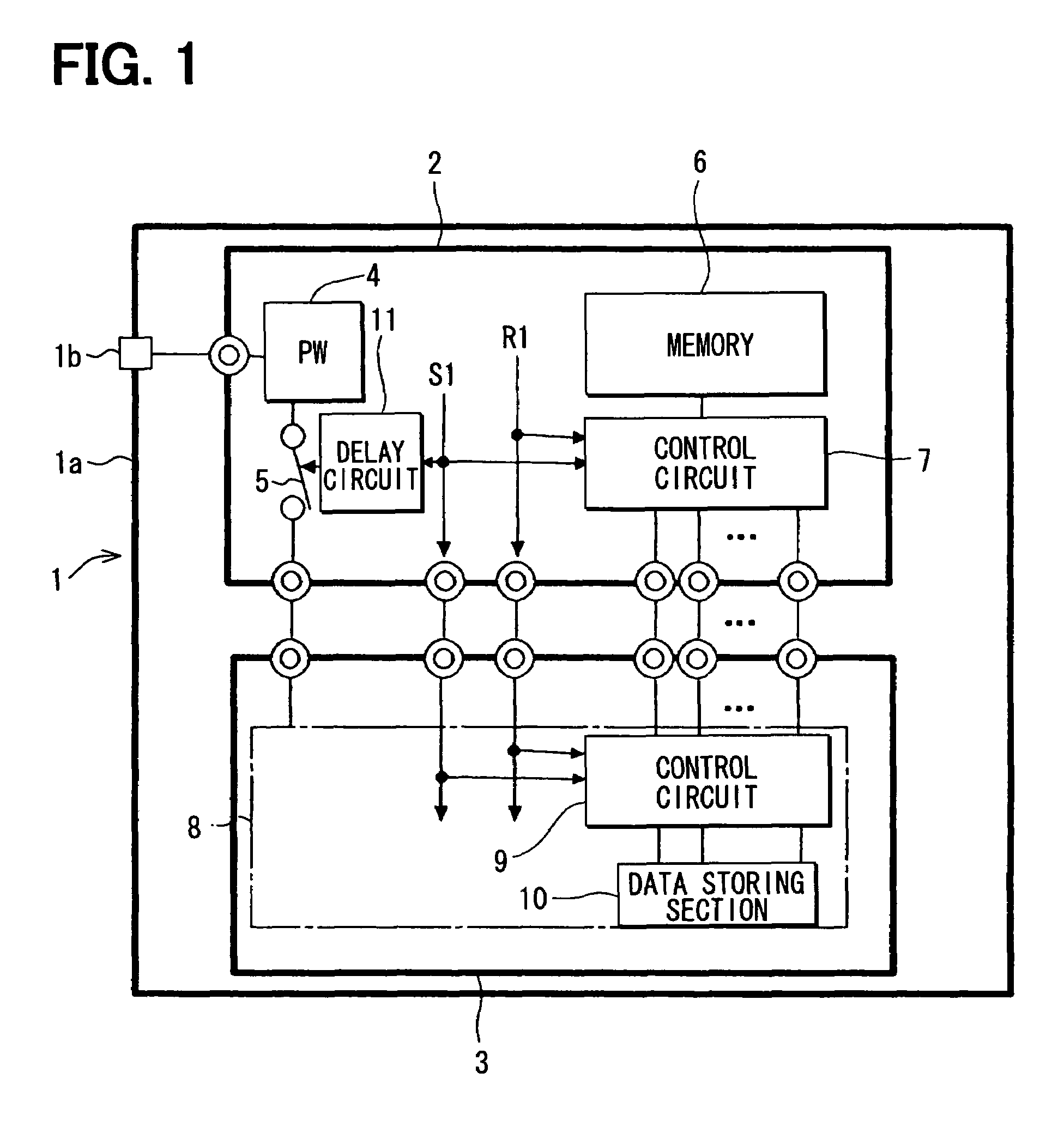
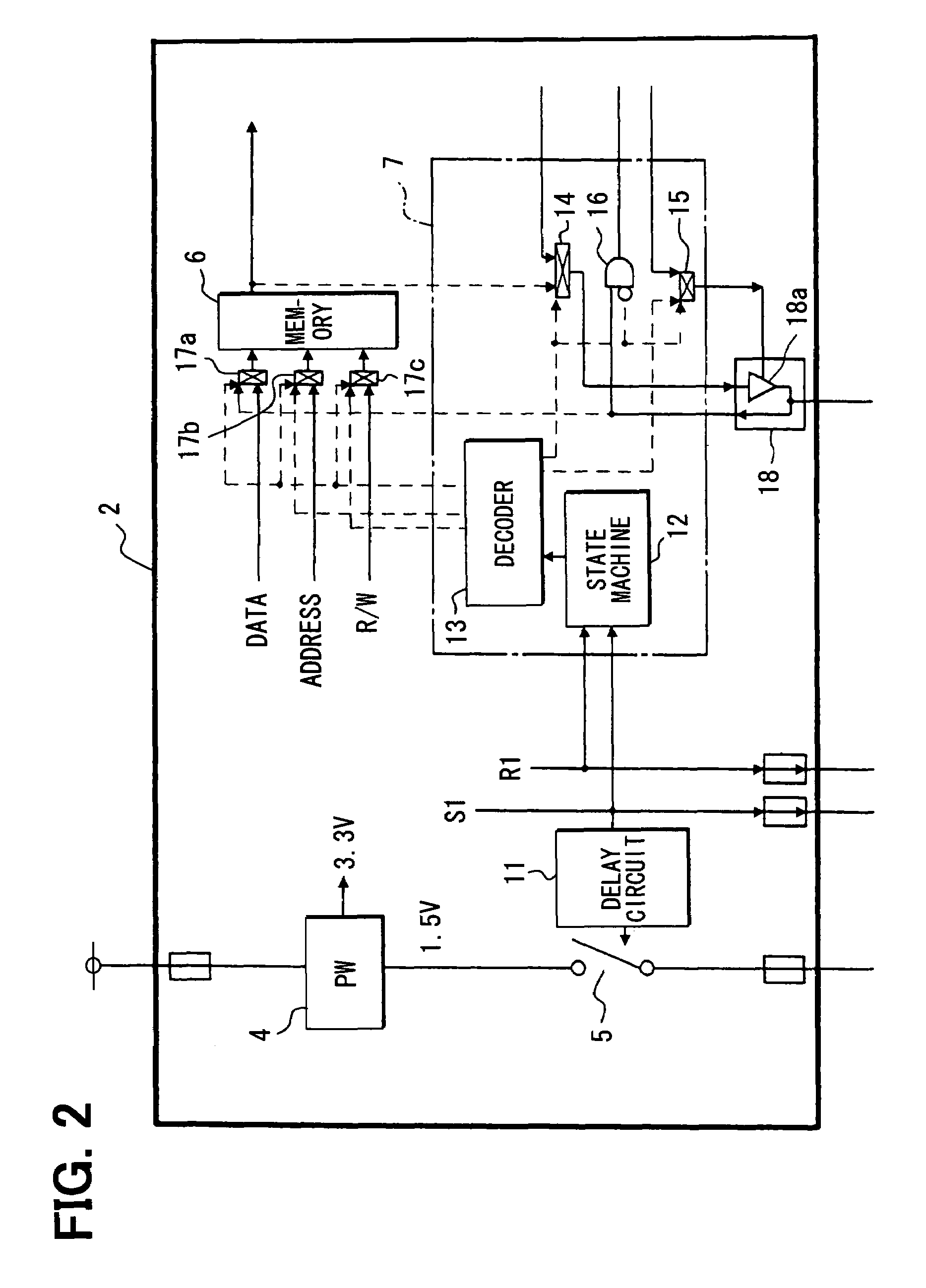
[0019]As shown in FIG. 1, a microcomputer 1 according to an embodiment of the present invention includes a package 1a and first and second chips 2, 3 received in the package 1a. The first and second chips 2, 3 are manufactured with different manufacturing processes such that a first leak current in the first chip 2 is less than a second leak current in the second chip 3. Typically, the manufacturing process is denoted by a minimum line-width on the integrated circuits. For example, the first chip 2 is manufactured with a 350 nm manufacturing process and operates at a first voltage of 3.3 volts (V). The second chip 3 is manufactured with a 150 nm manufacturing process and operates at a second voltage of 1.5 V. In short, the first chip 2 has a first integration degree less than a second integration degree of the second chip 3 and has a first minimum line-width greater than a second minimum line-width of the second chip 3. Therefore, for example, a metal-oxide semiconductor field-effec...


PUM


Abstract

A microcomputer having a sleep mode includes first and second chips received in a single package. The first and second chips are manufactured with different manufacturing processes such that a leak current in the first chip is less than that in the second chip. When a sleep signal for putting the microcomputer in the sleep mode becomes active, data stored in the second chip is transmitted to the first chip. After the data transmission is completed, a power supply voltage supplied to the second chip is stopped and the second chip stops its operation until the sleep mode is released. The data transmission is achieved by digital logic circuits that can be easily redesigned by using a conventional automatic layout generator.

Description

CROSS REFERENCE TO RELATED APPLICATION[0001]This application is based on and incorporates herein by reference Japanese Patent Application No. 2006-48468 filed on Feb. 24, 2006.FIELD OF THE INVENTION[0002]The present invention relates to a microcomputer including a first chip that continues operation in a sleep mode and a second chip that stops operation in the sleep mode.BACKGROUND OF THE INVENTION[0003]Typically, an integrated circuit (IC) such as a microcomputer has a sleep mode (i.e., low power consumption mode) that reduces power consumption. The sleep mode stops supply of clock signals to most of logic circuits in the IC so that the logic circuits stop operation.[0004]A manufacturing process technology of the IC is advanced and the IC is manufactured with a finer (e.g., 90 nm) manufacturing process. In other words, the number of transistors per chip is increased so that the transistors have a reduced minimum line-width. Such an IC operates at a lower voltage and the transistors...

Claims


Application Information

Patent Timeline
Patent Type & Authority Patents(United States)
IPC IPC(8): H01L23/48
CPCG06F1/3203G06F1/3243G06F1/3293G06F1/3296G11C5/148Y02B60/121Y02B60/1239Y02B60/1285Y02B60/32H01L2924/0002H01L2924/00Y02D10/00Y02D30/50
Inventor YAMADA, KENJIKOBAYASHI, CHIKARA
Owner DENSO CORP
Learn More