Method of manufacturing thin film transistor

a thin film transistor and manufacturing method technology, applied in the direction of electrical equipment, semiconductor devices, instruments, etc., can solve the problems of deteriorating yield, disconnection of electrodes formed in the subsequent process, degradation of liquid crystal display quality, etc., to achieve high yield, high carrier mobility, and high uniformity

Inactive Publication Date: 2006-03-14
VISTA PEAK VENTURES LLC
View PDF16 Cites 12 Cited by
  • Summary
  • Abstract
  • Description
  • Claims
  • Application Information

AI Technical Summary

Benefits of technology

[0018]It is therefore an object of the present invention to provide a method of manufacturing a TFT which can provide a clean interface between polysilicon and silicon oxide, which can thereby achieve high carrier mobility and high uniformity thereof without any overhang part formed in an island forming process, and which can accomplish a high yield.

Problems solved by technology

Such a step results in disconnection of electrodes formed in the subsequent process or deterioration of yield due to a leak current flowing between the electrodes and the semiconductor film 103.
This brings about degradation of the quality of liquid crystal displays when such an undulated transparent insulating substrate 101 is used.
Therefore, there is a disadvantage that disconnection or connection failures of electrodes unfavorably take place and thus the yield is deteriorated because of defective transistors.
However, there still exists a disadvantage that contamination is not avoidable on the surface of the semiconductor film 103 because the semiconductor film 103 is not covered until the second gate oxide film 108 is formed.

Method used


Image

  • Method of manufacturing thin film transistor
  • Method of manufacturing thin film transistor
  • Method of manufacturing thin film transistor

Examples


embodiments

[0040]Firstly, description will be made about a method of manufacturing a TFT, which is one embodiment of the present invention.

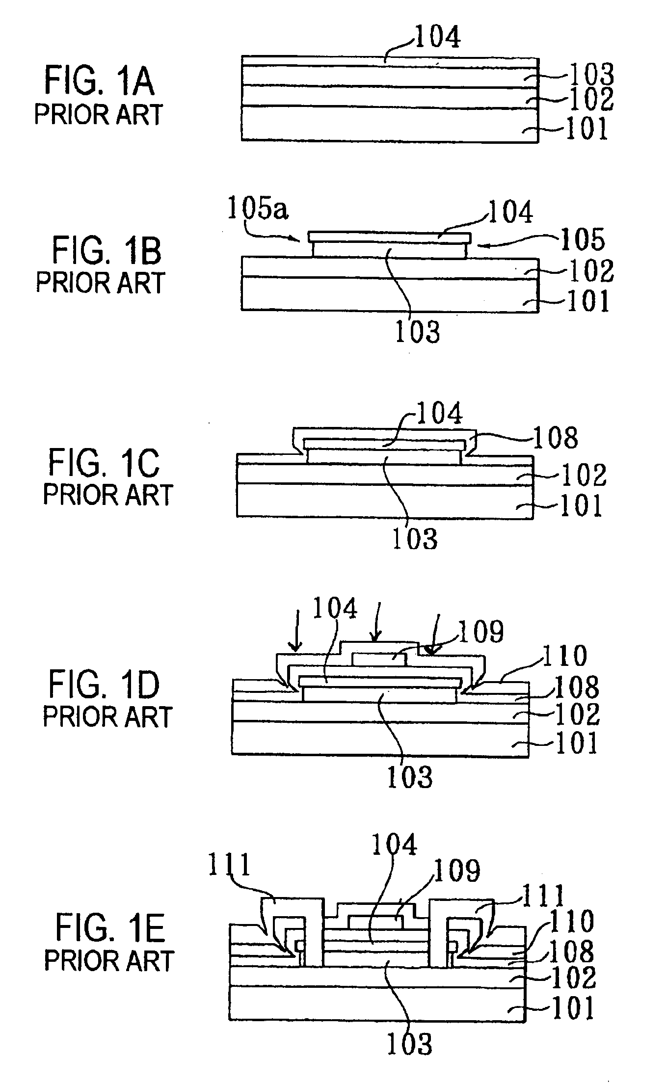
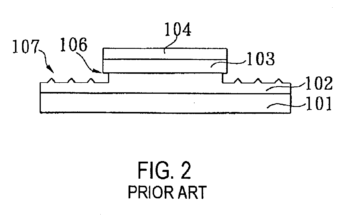
[0041]In the method of manufacturing a TFT according to the embodiment, a first insulating film is formed in a first insulating film forming process on a semiconductor film which is formed on a substrate, and then the semiconductor film and the first insulating film are patterned into island shape in an island forming process. Thereafter, an overhang part removal process or a cleaning process is carried out. In the overhang part removal process or the cleaning process, the overhang part, where a side end part of the first insulating film making the island is formed into a visor shape over a side end part of the semiconductor film, is removed. After this, a second insulating film is formed on the island in the second insulating film forming process, and a gate electrode is formed on the second insulating film in a gate electrode forming process.

[0042]This al...

first embodiment

[0043]Next, a method of manufacturing a TFT will be described with reference to drawings according to a first embodiment of the present invention.

[0044]FIGS. 1 and 2 are process diagrams illustrating the method of manufacturing a TFT according to the first embodiment of the present invention, FIG. 5 is a schematic diagram of a constitution of a TFT manufacturing apparatus which is used for manufacturing the TFT and in which film deposition and laser irradiation to the transparent insulating substrate are performed, and FIG. 6 is a schematic diagram of a constitution of a spin cleaning apparatus used for manufacturing the TFT.

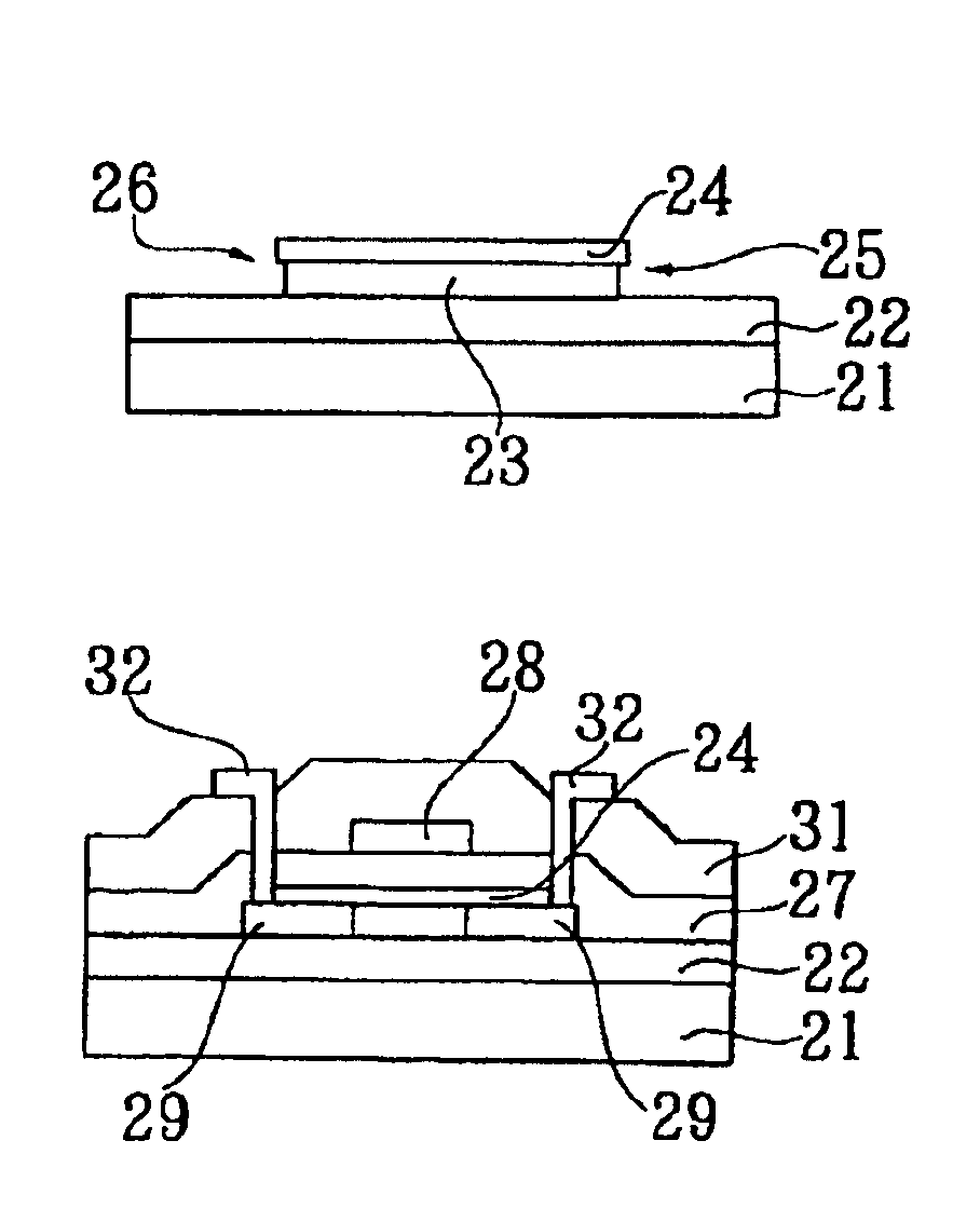
[0045]In the method of manufacturing the TFT in this example, prepared is a transparent insulating substrate (substrate) 1 made of glass which is cleaned by ultrasonic cleaning or the like, for example, OA-10 of Nippon Electric Glass Co., Ltd, as shown in FIG. 1A. Next, the transparent insulating substrate 1 is introduced into the TFT manufacturing apparatus 2 f...

second embodiment

[0083]FIG. 7 is a process diagram illustrating a method of manufacturing a TFT, which is a second embodiment of the present invention.

[0084]The example here is considerably different from the first embodiment in that, in contrast that the film deposition and the laser irradiation to the transparent insulating substrate are performed in the TFT manufacturing apparatus without exposing the transparent insulating substrate to the outside air, such film deposition and laser irradiation are performed in different apparatus, and that the transparent insulating substrate having the island part is only immersed in the aqueous hydrofluoric acid solution in substitution for the spin-cleaning in the cleaning / overhang part removal process.

[0085]The constitution other than this is substantially the same as that of the first embodiment described above, and explanation thereof will thus be simplified.

[0086]In this example, the film deposition of the underlying protection film and the semiconductor...


PUM

PropertyMeasurementUnit
temperatureaaaaaaaaaa
pressureaaaaaaaaaa
temperatureaaaaaaaaaa

Abstract

After a polysilicon semiconductor film 5 and a first gate oxide film 6 are formed on a transparent insulating substrate 1, the semiconductor film 5 and the first gate oxide film 6 are patterned into an island shape to form an island part. At this time, an overhang part 8 of a visor shape is formed where side end surfaces of the first gate oxide film 6 and the semiconductor film 5 are not aligned and an end part of the first gate oxide film 6 projects slightly from a position of a side end surface of the semiconductor film 5. The overhang part 8 is removed, for example, during cleaning, which thus enhances yield.

Description

BACKGROUND OF THE INVENTION[0001]1. Field of the Invention[0002]The present invention relates to a method of manufacturing a thin film transistor (hereinafter referred to as TFT) of a top gate type, which is, for example, used as a switching element and the like in a liquid crystal display or organic EL (Electroluminescent) display and is formed of polysilicon on an insulating substrate.[0003]2. Description of the Related Art[0004]A liquid crystal display is manufactured, for example, by encapsulating liquid crystals into a clearance between a TFT substrate and a CF (Color Filter) substrate to make a liquid crystal display panel, thereafter connecting it to a TCP (Tape Carrier Package) mounted with a drive IC for driving the liquid crystal display panel and further connecting the TCP to a wiring board for supplying signals and power.[0005]In recent years, reduction of a size and thickness has been required in a liquid crystal display of an active matrix type. To this end, several at...

Claims


Application Information

Patent Timeline
Patent Type & Authority Patents(United States)
IPC IPC(8): H01L21/335H01L21/8232G02F1/1368H01L21/20H01L21/308H01L21/336H01L29/49H01L29/786
CPCH01L29/66757H01L29/4908H01L29/786
Inventor OKUMURA, HIROSHISHIOTA, KUNIHIRO
Owner VISTA PEAK VENTURES LLC
Why Eureka
Try Eureka