Self-aligned differential oxidation in trenches by ion implantation

a technology of differential oxidation and trenches, which is applied in the direction of semiconductor devices, basic electric elements, electrical appliances, etc., can solve the problems of reducing the internal capacitance of mosfets, increasing the current carrying capacity, and reducing the on-resistance of devices, so as to increase reduce the growth rate of insulating layers

Inactive Publication Date: 2006-03-14
SILICONIX
View PDF27 Cites 21 Cited by
  • Summary
  • Abstract
  • Description
  • Claims
  • Application Information

AI Technical Summary

Benefits of technology

[0006]In accordance with the present invention, a trench MOSFET is formed by creating a trench in a semiconductor substrate. A portion of either a side wall of the trench, or the bottom of the trench, or both the side wall and bottom, is implanted with an implant species. An insulating layer is then grown overlying the bottom and side wall of the trench. The implant species is selected such that the insulating layer grows more quickly on the bottom of the trench than on the side wall of the trench, resulting in a thicker insulating layer in the bottom of the trench than on the trench side walls. In some embodiments, a first implant species is implanted in the bottom of the trench and a second species is implanted in the side wall of the trench. The first implant species is selected to increase the insulating layer growth rate and the second implant species is selected to decrease the insulating layer growth rate. In some embodiments, the first implant species is argon, neon, arsenic, or an inert gas. In some embodiments, the second implant species is nitrogen.

Problems solved by technology

All else being equal, this increases the current carrying capability and reduces the on-resistance of the device.
One of the most important issues for high frequency operation, however, is reduction of the MOSFET internal capacitances.
The large overlap limits the drain voltage rating of MOSFET 10, presents long term reliability issues for thin gate insulator 15, and greatly increases the gate-to-drain capacitance, Cgd, of MOSFET 10.

Method used


Image

  • Self-aligned differential oxidation in trenches by ion implantation
  • Self-aligned differential oxidation in trenches by ion implantation
  • Self-aligned differential oxidation in trenches by ion implantation

Examples


Embodiment Construction

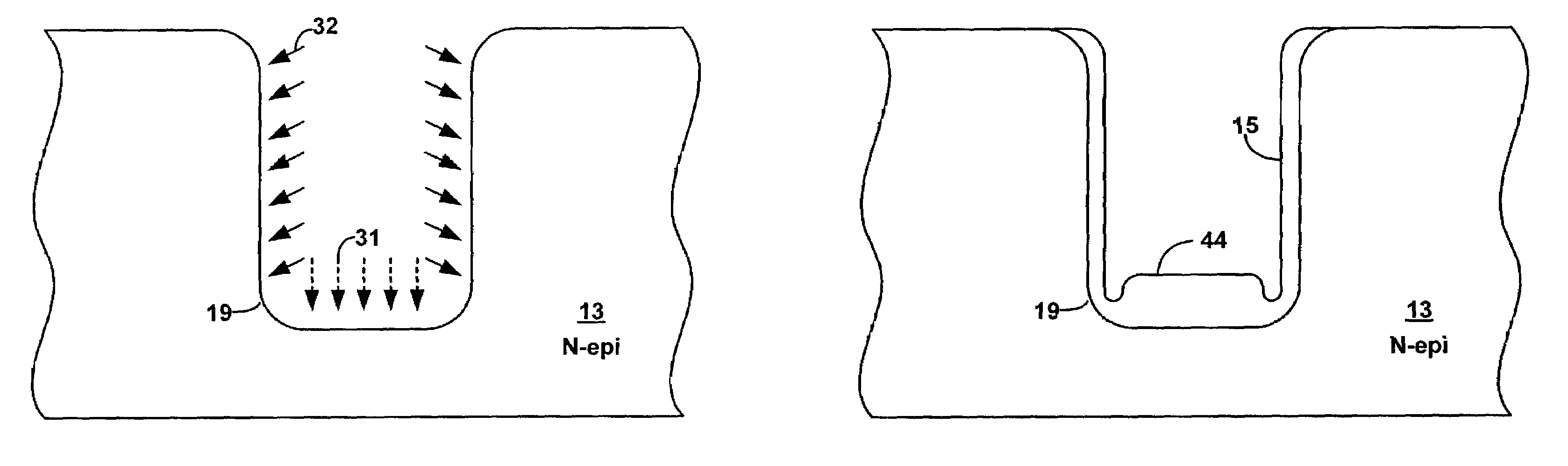
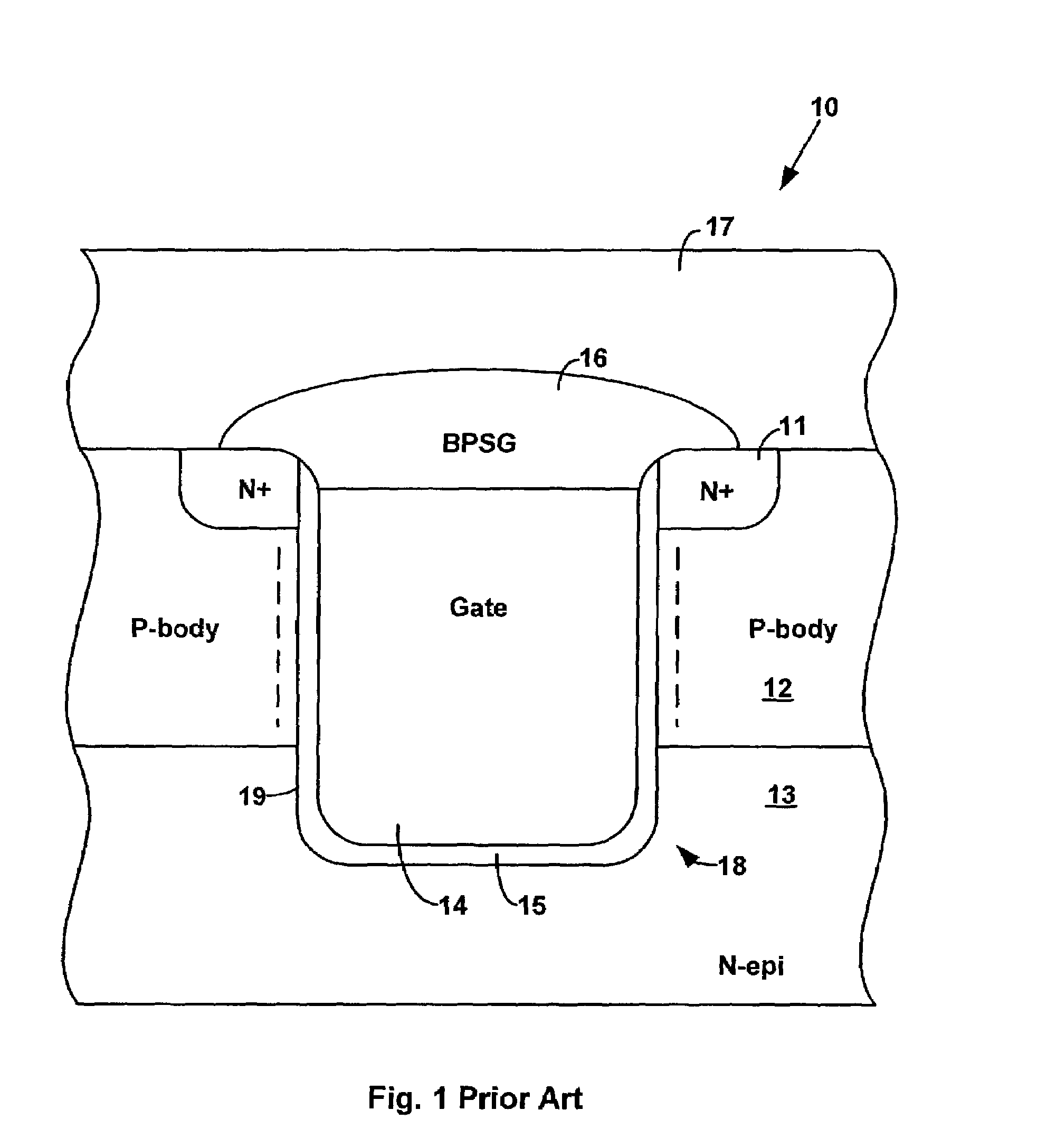
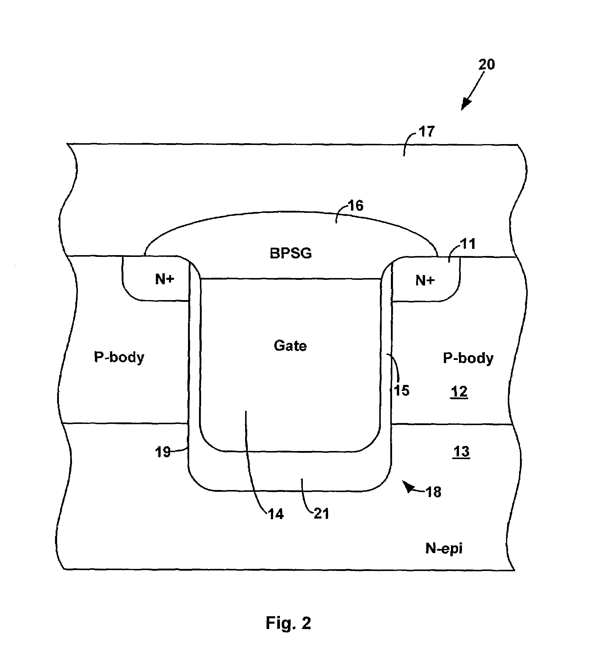
[0012]FIG. 2 is a cross sectional view of one embodiment of a trench MOSFET 20 in accordance with the present invention. In MOSFET 20, an n-type epitaxial layer 13, which may be an N− layer and is usually grown on an N+ layer (not shown), forms the drain of the MOSFET. A p-type body layer 12 separates the N-epi layer 13 from N+ source regions 11. Body region 12 is diffused along the side wall of a trench 19. Polysilicon gate 14 is formed in trench 19. The side walls of trench 19 are lined with a thin gate insulator 15 (for example, silicon dioxide). A thick insulating layer 21 (for example, silicon dioxide) lines the bottom of trench 19 in MOSFET 20. Thick insulating layer 21 separates gate 14 from N-epi layer 13 (the drain). Thick insulating layer 21 provides a more effective insulator than is achievable with the thin insulating layer 15 lining the bottom of trench 19 in FIG. 1. Thus, thick insulating layer 21 minimizes the gate-to-drain capacitance and yields a trench MOSFET 20 us...


PUM


Abstract

In accordance with the present invention, a trench MOSFET is formed by creating a trench in a semiconductor substrate. A portion of either a side wall of the trench or the bottom of the trench is implanted with an implant species. An insulating layer is then grown overlying the bottom and side wall of the trench. The implant species is selected such that the insulating layer grows more quickly on the bottom of the trench than on the side wall of the trench, resulting in a thicker insulating layer in the bottom of the trench than on the trench side walls.

Description

CROSS REFERENCE TO RELATED APPLICATIONS[0001]This application is related to application Ser. No. 09 / 927,143, titled “Trench MIS Device With Active Trench Corners And Thick Bottom Oxide And Method Of Making The Same,” filed Aug. 10, 2001, and incorporated herein by reference.BACKGROUNDDescription of Related Art[0002]Some metal-insulator-semiconductor (MIS) devices include a gate located in a trench that extends downward from the surface of a semiconductor substrate (e.g., silicon). The current flow in such devices is primarily vertical and, as a result, the cells can be more densely packed than devices with lateral current flow. All else being equal, this increases the current carrying capability and reduces the on-resistance of the device. Devices included in the general category of MIS devices include metal-oxide-semiconductor field effect transistors (MOSFETs), insulated gate bipolar transistors (IGBTs), and MOS-gated thyristors.[0003]Trench MOSFETs, for example, can be fabricated...

Claims


Application Information

Patent Timeline
Patent Type & Authority Patents(United States)
IPC IPC(8): H01L21/336H01L21/265H01L21/28H01L29/08H01L29/423H01L29/78
CPCH01L29/7813H01L29/42368H01L21/2822H01L21/26506H01L21/26586H01L21/28211H01L29/0847H01L29/0878
Inventor LICHTENBERGER, KARLGILES, FREDERICK P.YUE, CHRISTIANATERRILL, KYLEDARWISH, MOHAMED N.PATTANAYAK, DEVALUI, KAM HONGXU, ROBERT Q.CHEN, KUO-IN
Owner SILICONIX
Why Eureka
Try Eureka