Semiconductor device having contact prevention spacer

a technology of contact prevention and semiconductor devices, which is applied in the direction of basic electric elements, material analysis, other domestic articles, etc., can solve the problems of causing short-circuits, deformation of the upper metallic mold, and so as to and reduce the risk of deformation of the metal wire

Inactive Publication Date: 2006-03-21
LAPIS SEMICON CO LTD
View PDF21 Cites 12 Cited by
  • Summary
  • Abstract
  • Description
  • Claims
  • Application Information

AI Technical Summary

Benefits of technology

[0025]According to the first aspect of the present invention, the contact prevention resin having a predetermined height is adhered to the surface of each of the semiconductor elements. As a result, even if the wiring substrate warps due to heating or the like, when the upper metallic mold for mold processing is placed on the wiring substrate, the inner surface of the upper metallic mold abuts against the contact prevention resin, and thus the metal wire is protected. Therefore, there is reduced risk of deforming the metal wire.
[0026]According to the second aspect of the present invention, the contact prevention protruding portion is formed at the inner side of the upper metallic mold for mold processing. As a result, even if the wiring substrate warps, the metal wire is protected by the protruding portion of the upper metallic mold when the upper metallic mold is placed on the wiring substrate. Accordingly, there is reduced risk of deforming the metal wire.
[0027]Further, in the second aspect of the present invention, the protruding portion provided inside of the upper metallic mold is preferably formed at a position corresponding substantially to the center of the semiconductor element bonded onto the wiring substrate in such a manner that the dimension of the protruding portion in a direction to which it protrudes is greater than a distance between the surface of the semiconductor element and the highest position of the metal wire connected to the semiconductor element, and is also smaller than the height of the mold resin injected onto the semiconductor element from the semicond

Problems solved by technology

However, the above-described structure of semiconductor devices and method for producing the same, which have been conventionally known, have the following problems.
When the upper metallic mold is placed on the wiring substrate in the above-de

Method used


Image

  • Semiconductor device having contact prevention spacer
  • Semiconductor device having contact prevention spacer
  • Semiconductor device having contact prevention spacer

Examples


first embodiment

[First Embodiment]

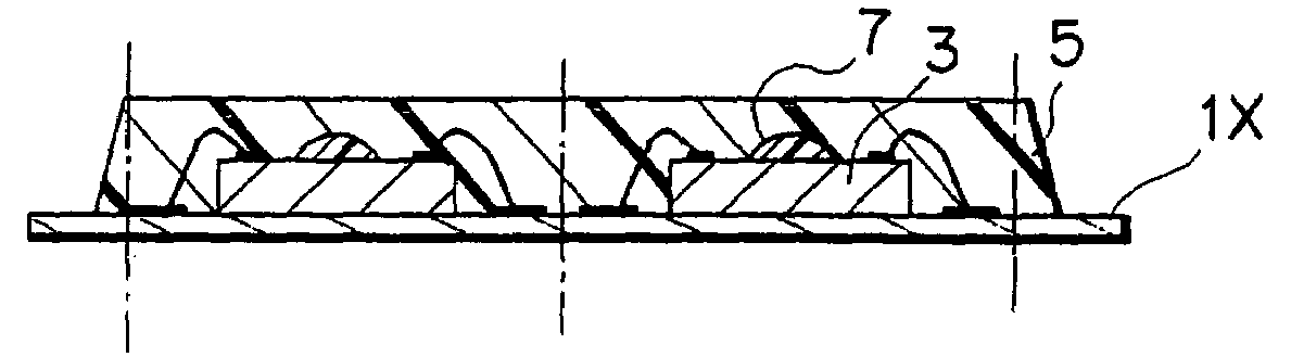
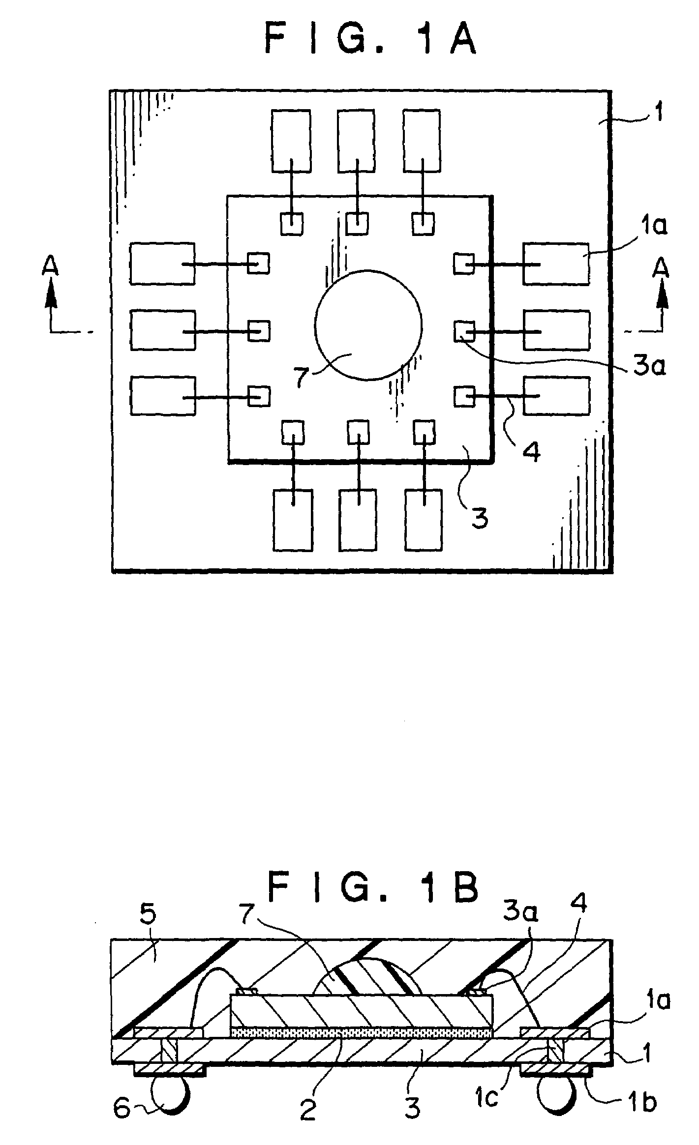
[0035]FIGS. 1A and 1B are each a structural diagram of a semiconductor device according to a first preferred embodiment of the present invention. FIG. 1A is a plan view and FIG. 1B is a cross sectional view taken along the line A—A in FIG. 1A. In FIGS. 1A and 1B, the same members as those in FIG. 2 are denoted by the same reference numerals.

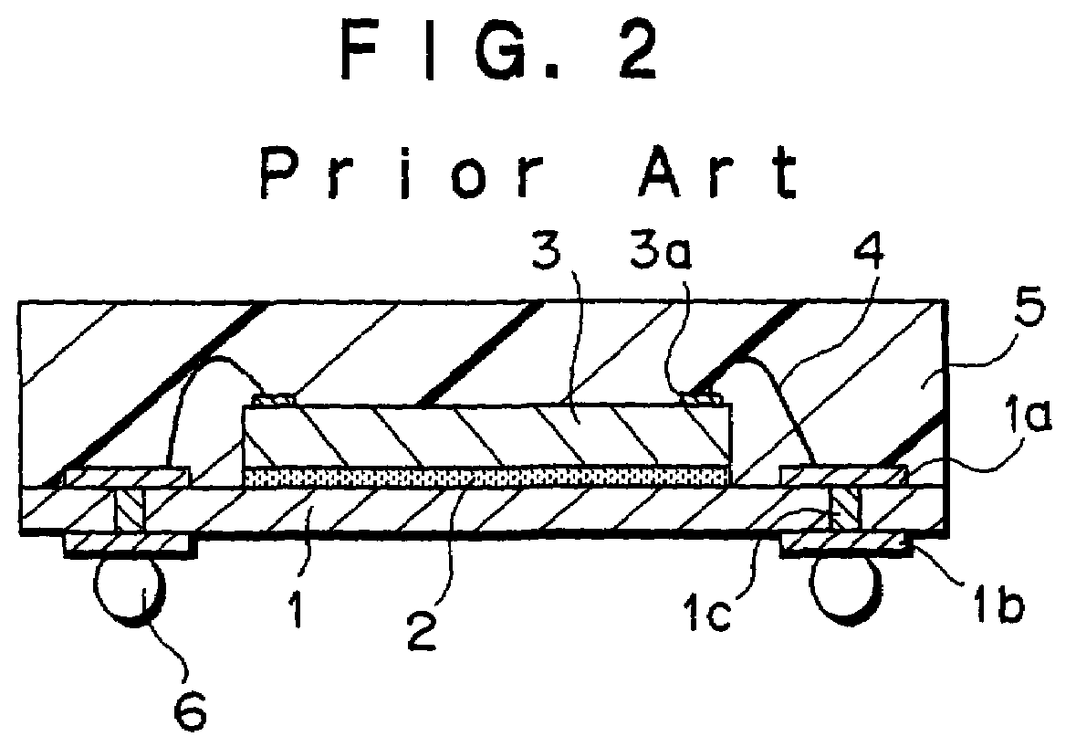
[0036]The semiconductor device shown in FIGS. 1A and 1B is that of BGA / CSP type produced by package molding / saw cutting techniques. A semiconductor element 3 (for example, an IC chip) is fixed onto a wiring substrate 1 by an adhesive agent 2. The wiring substrate 1 is formed of, for example a glass / epoxy substrate having a thickness of 0.2 mm or thereabouts and transverse and vertical dimensions of approximately 5 to 15 mm. Wiring patterns 1a and 1b are respectively formed on face and reverse surfaces of the wiring substrate 1 in the periphery thereof. Further, the wiring patterns 1a and 1b are electrically connected to each oth...

second embodiment

[Second Embodiment]

[0045]FIGS. 4A to 4C are explanatory diagrams showing a method for producing a semiconductor device according to a second preferred embodiment of the present invention. It should be noted that the same members as those in FIGS. 3A to 3C will be denoted by the same reference numerals.

[0046]In the above-described production method shown in FIGS. 3A to 3C, the contact prevention resin 7 adheres to the surface of the IC chip 3 so as to prevent the wire 4 from contacting the inner surface of the upper metallic mold 12. In comparison, in the production method shown in FIGS. 4A to 4C, an upper metallic mold 12A is used which has contact prevention protruding portions 12a formed at the inner side of the upper metallic mold at positions corresponding to respective central portions on the surfaces of the IC chips 3.

[0047]Referring now to FIGS. 4A to 4C, the method for producing a semiconductor device according to the second embodiment will be described hereinafter.

[0048]As ...

third embodiment

[Third Embodiment]

[0055]FIGS. 5A to 5C are explanatory diagrams showing a method for producing a semiconductor device according to a third preferred embodiment of the present invention. Note that the same members as those in FIGS. 4A to 4C will be denoted by the same reference numerals.

[0056]The production method shown in FIGS. 5A to 5C is different from the production method shown in FIGS. 4A to 4C in the position and dimensions of the contact prevention protruding portion formed at the inner side of the upper metallic mold.

[0057]That is, the upper metallic mold 12A shown in FIG. 4B has the contact prevention protruding portions 12a on the inner surface of the upper metallic mold 12A at the positions corresponding to the respective central portions on the surfaces of the IC chips 3 so as to prevent the wire 4 from contacting the inner surface of the upper metallic mold 12A. On the other hand, an upper metallic mold 12B shown in FIG. 5B has a warp prevention protruding portion 12b f...


PUM

PropertyMeasurementUnit
Heightaaaaaaaaaa
Deformation enthalpyaaaaaaaaaa

Abstract

There is provided a semiconductor device in which substantially no deformation of a bonded wire occurs, and a method for producing the semiconductor device. A wiring pattern of a wiring substrate and an electrode of an IC chip are connected by a wire. A contact prevention resin whose height is higher than the highest position of the bonded wire, is adhered to the approximate center of the surface of the IC chip. If the wiring substrate warps due to heat from the lower metallic mold, an inner surface of an upper metallic mold placed on the wiring substrate abuts against the contact prevention resin, and decrease warpage of the wiring substrate. Accordingly, the wire is kept from contacting the inner surface of the upper metallic mold. Thereafter, the IC chips, the wires, and the like are sealed by injecting a mold resin into the molds.

Description

[0001]This application is a divisional of U.S. application Ser. No. 09 / 716,463, filed Nov. 21, 2000, now U.S. Pat. No. 6,624,058.BACKGROUND OF THE INVENTION[0002]1. Field of the Invention[0003]The present invention relates to a resin seal type semiconductor device, and a method for producing the same.[0004]2. Description of the Related Art[0005]Recently, in keeping with the tendency toward high density packaging of electrical appliances, there has been increased demand for thin and small-sized semiconductor devices, and the production quantity of resin seal type packages such as Ball Grid Array / Chip Size Package (BGA / CSP) has increased. In these circumstances, in order to improve BGA / CSP production or the like, a production method using package molding / saw cutting techniques has been widely used where a plurality of integrated circuit (IC) chips are fixed to one wiring substrate and sealed all together by mold resin. Thereafter, the wiring substrate is cut into separate semiconducto...

Claims


Application Information

Patent Timeline
IPC IPC(8): H01L23/28H01L23/29B29C45/14B29L31/34H01L21/56H01L23/12H01L23/16H01L23/31
CPCH01L21/561H01L23/16H01L23/3128H01L24/97H01L21/565Y10T436/179228H01L2224/48091H01L2224/48227H01L2224/49175H01L2224/73265H01L2224/97H01L2924/01004H01L2924/01079H01L2924/14H01L2924/15311H01L2224/45144H01L24/49H01L2924/1815H01L2224/32225H01L2924/01033H01L2924/01006H01L2924/01005H01L24/48H01L2224/85H01L2924/00014H01L2924/00H01L2924/00012H01L24/45H01L24/73H01L2224/05554H01L2924/181H01L2224/45015H01L2924/207
Inventor KAZAMA, TAKAO
Owner LAPIS SEMICON CO LTD
Why Eureka
Try Eureka