

Semiconductor substrate having pillars within a closed empty space
a technology of semiconductor substrate and empty space, which is applied in the direction of optical elements, instruments, optical waveguide light guides, etc., can solve the problems of large cost, inability to obtain sufficient reliability, and inability to form a soi substrate suitable for a household electronic device such as a dram, so as to achieve the effect of not raising the cost or deteriorating the reliability
- Summary
- Abstract
- Description
- Claims
- Application Information
AI Technical Summary
Benefits of technology
Problems solved by technology
Method used
Image

Examples
first embodiment
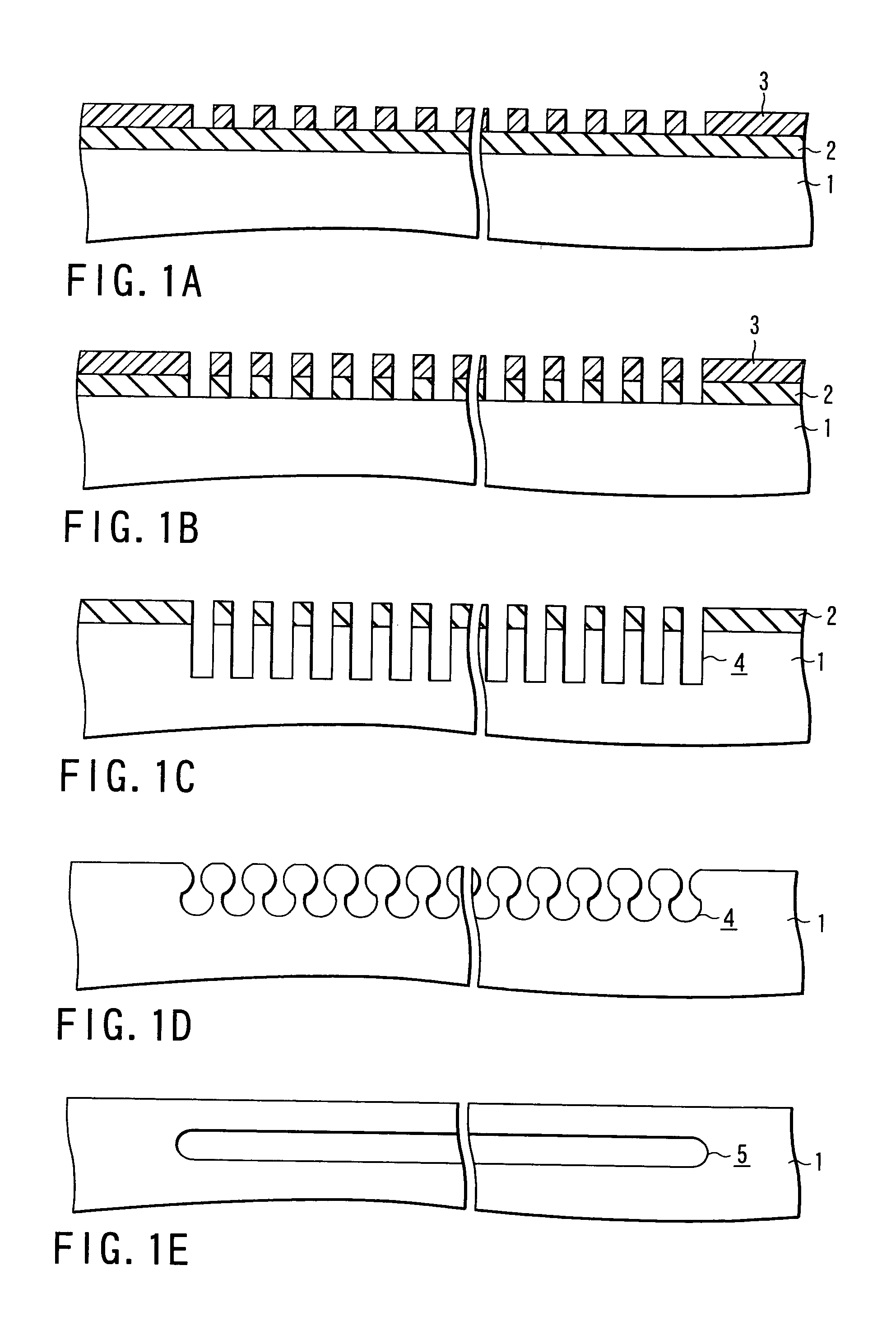
[0072]FIGS. 1A to 1E are sectional views showing a method for fabricating a silicon substrate having a flat empty space (ESS: Empty Space in Silicon) of the first embodiment of the present invention, that is, an SON (Silicon On Nothing) substrate referred to as an ultimate SOI substrate.
[0073]First, as shown in FIG. 1A, a mask material 2 is formed on a single-crystal silicon substrate 1 and a photoresist pattern 3 is formed on the mask material 2. The mask material 2 will be described later.
[0074]Then, as shown in FIG. 1B, the mask material 2 is patterned through anisotropic etching such as RIE by using the photoresist pattern 3 as a mask to transfer the pattern of the photoresist pattern 3 to the mask material 2.
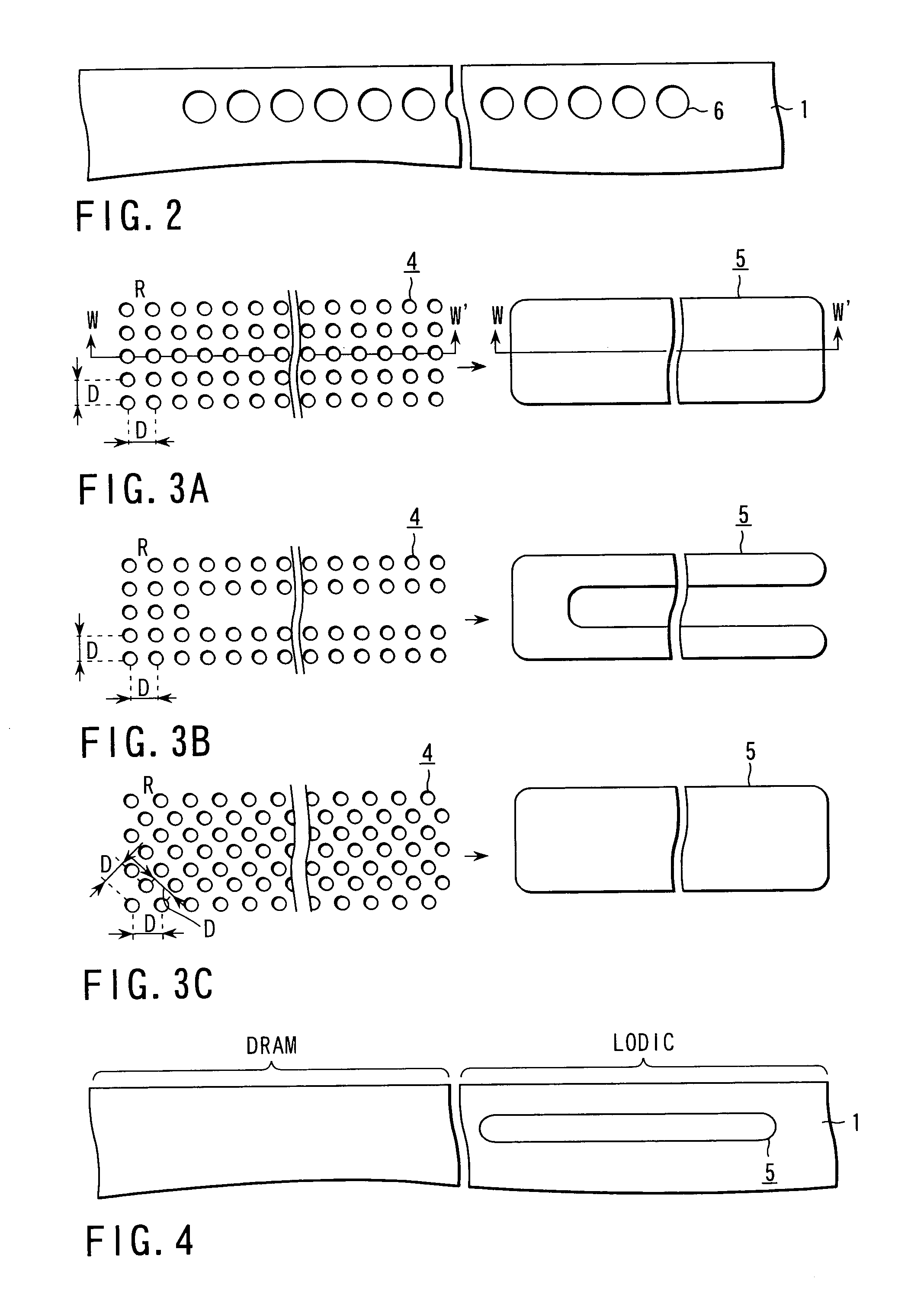
[0075]Then, as shown in FIG. 1C, the photoresist pattern 3 is carbonized and separated and then, the silicon substrate is patterned through anisotropic etching such as RIE by using the mask material 2 as a mask to two-dimensionally arrange a plurality of trenches 4 on the s...
second embodiment
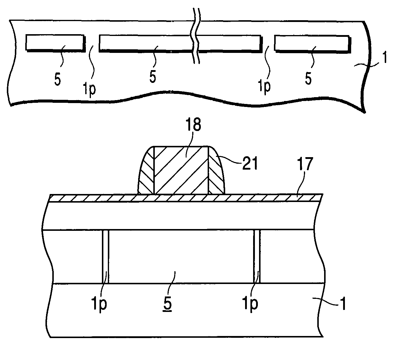
[0103]FIGS. 5A to 5L are sectional views showing a method for fabricating a MOS transistor of the second embodiment of the present invention. In the following drawings, a symbol same as that in a previous drawing shows the same or a corresponding portion and its detailed description is omitted.
[0104]For this embodiment, a case is described in which a flat empty space is formed in a silicon substrate to fabricate a MOS transistor on the flat empty space.
[0105]First, a flat empty space 5 is formed in a silicon substrate 1 as shown in FIG. 5A in accordance with the same method as the case of the first embodiment shown in FIGS. 1A to 1E.
[0106]Then, as shown in FIG. 5B, a silicon oxide film 7, a silicon nitride film 8, and a photoresist pattern 9 are formed in order on the silicon substrate 1.
[0107]In this case, the photoresist pattern 9 is laid out so that at lest a part of the opening of the pattern 9 is brought onto an empty space forming region. FIG. 5B shows a case in which the patt...
third embodiment
[0127]FIGS. 6A to 6D are sectional views showing a method for fabricating a MOST transistor of the third embodiment of the present invention. For the second embodiment, a method for filling a flat empty space with a silicon oxide film is described. For the third embodiment, however, a method for leaving a flat empty space without filling the empty space with a silicon oxide film is described.
[0128]First, as shown in FIG. 6A, a flat empty space 5 is formed in a silicon substrate 1 in accordance with the method used for the first embodiment shown in FIGS. 1A to 1E.
[0129]Then, as shown in FIG. 6B, a silicon thermal oxide film 24 is formed in the flat empty space 5 and on the surface of the silicon substrate through thermal oxidation. The above thermal oxidation is performed, for example, in a mixed gas of oxygen and HCl at 900° C. A silicon thermal oxide film 22 serves a stopper under RIE as shown in FIG. 5G in subsequent steps.
[0130]Then, as shown in FIG. 6C, a silicon nitride film 25...
PUM
 Abstract
Description
Claims
Application Information