Nonvolatile memory device and method for fabricating the same

a memory device and non-volatile technology, applied in semiconductor devices, digital storage, instruments, etc., can solve the problems of unerased bit or second bit effect, indicating charge loss, and disadvantages of conventional sonos flash memory, and achieve the effect of efficient erase operation

Inactive Publication Date: 2006-03-28
SOLID STATE SYST
View PDF3 Cites 28 Cited by
  • Summary
  • Abstract
  • Description
  • Claims
  • Application Information

AI Technical Summary

Benefits of technology

[0015]The invention provides a non-volatile memory device, which can have efficient erase operation without causing much residue charges in the charge storage layer.
[0016]The invention provides a non-volatile memory device, which has selection gate design with capability to effectively prevent the bit error from occurring. Therefore, the charges can be well localized at the desired location. Also and, the selection gate can create a low program current and high program efficiency.

Problems solved by technology

However, the conventional SONOS flash memory has the disadvantages.
Although the charge trapped in nitride or other discrete comparing to charges in conductor film, the charges still drift at high temperature for a long period, indicating charge loss.
Further, due to the unlimited storage region caused by the nitride on the whole channel, the program and erase region can not overlap properly and also results in un-erased bit or second bit effect.
In addition, the conventional hot carriers with low injection efficiency for programming consumes a larger current that can't support page mode programming.
Due to low mobility for the carriers in the nitride layer, the electrons and the holes are not fully neutralized with respect to the position.
Then, it would cause the read error due to the residual charges.
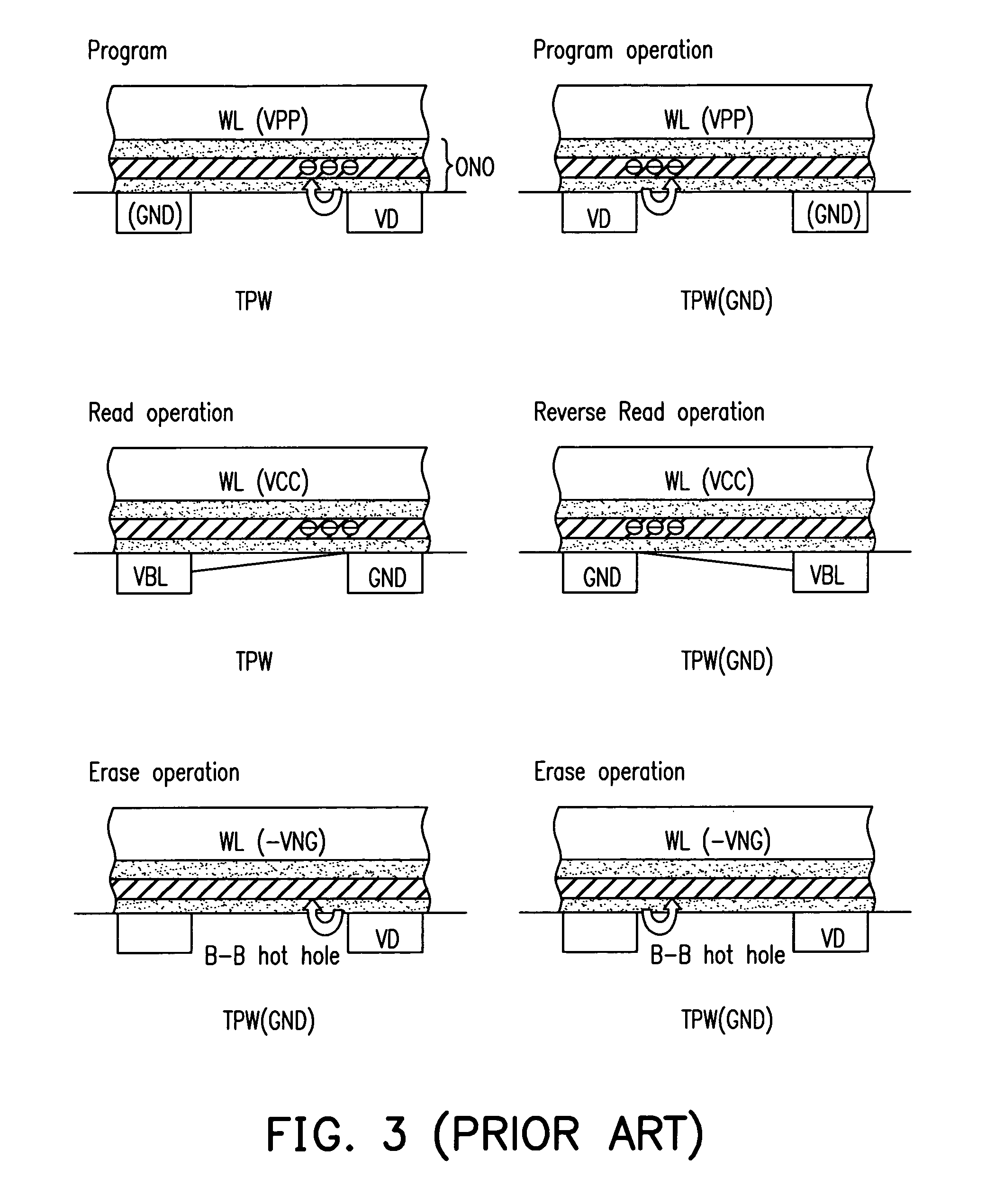
However, in this situation, after the erase operation, the residual positive holes stay in the nitride layer.
It would cause the error for the next programming operation.
In other words, the conventional structure in FIG. 4A has the issue in read error and programming error.
It then causes a failure of the memory cell.
Also and, the operation voltages are not stable for each time of operations.
When the erased cell is programmed again, however, electrons are difficult to inject to the storage layer over BL junction because the high electrical field distributes on the interface of select transistor and memory transistor.
After several P / E cycling, it may cause a peak of holes piling up on the storage layer near the BL junction.
Another impact of the pile-up of holes is to cause the potential failure of data retention.
The migration of holes will decrease the threshold voltage of program or erase cell, indicating the poor retention performance.
On the other hand, such a memory is not allowed to over erase according to its array structure.
Besides, once the cell is over erased, the BL to BL leak will be serious to make the error bit.

Method used


Image

  • Nonvolatile memory device and method for fabricating the same
  • Nonvolatile memory device and method for fabricating the same
  • Nonvolatile memory device and method for fabricating the same

Examples


embodiment 1

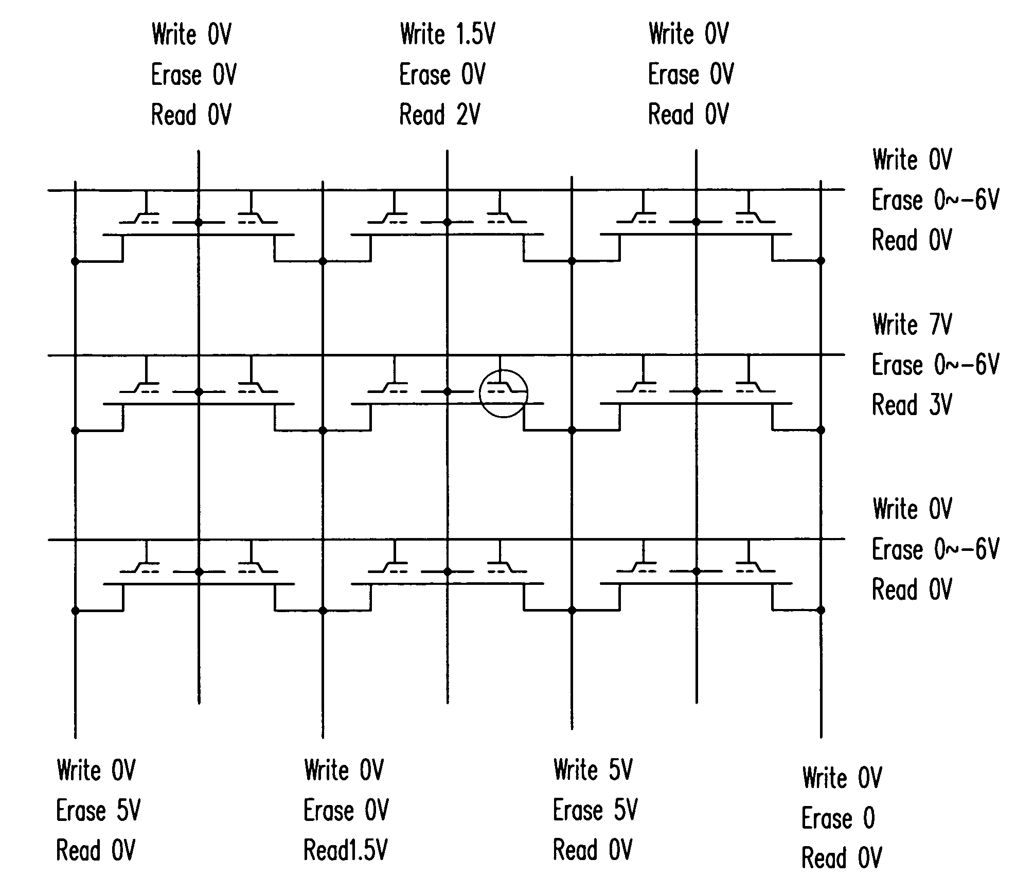
[0054]In the invention, a novel structure of non-volatile memory is proposed. First referring to FIGS. 5A–5C, which are cross-sectional views and top views, and a simplified circuit, schematically illustrating a structure of non-volatile memory device, according to an embodiment of the invention. In FIG. 5A, the buried bit line BL 1402 is formed in the substrate 1306. A gate structure with the selection gate SG is disposed on the substrate 1306 between two bit lines 1402. The gate structure can include the gate insulating layer between the selection gate SG and the substrate 1306. A cap layer can, for example, further be included at top of the selection gate SG. The oxide layer 1308 of the O / N / O charge storage structure layer is formed at least at the sidewall of the gate structure and on the substrate between the selection gate and the bit line 1402. The L-shape charge storage layers 1404′ and 1404″, such as nitride layers, are formed ate the sidewall of the gate structure, another...

embodiment 2

[0079]In the invention, further a novel structure of non-volatile memory is proposed. In the invention, selection gate (SG) lines are for example in the middle of a memory cell with separated two charge storage films over the substrate between the bit line and SG line, and preferably also on the sidewall of the SG line. A pocket doped region is formed in the substrate about under the sidewall of the selection gate. In operation, when the selection gate lines are applied a voltage, the substrate at the corresponding region becomes an inversion region, which can serve as a S / D region. In this design, the storage charges can be well localized to the desired region in the charge storage layer, such as the nitride layer. Embodiments with drawings are used as the example for descriptions.

[0080]FIG. 14A is one cross-sectional along the word line, schematically illustrating a novel non-volatile memory, such as flash memory, according to an embodiment of the invention. Basically, the memory ...


PUM


Abstract

A structure of non-volatile memory has a plurality of buried bit lines in a substrate, extending along a first direction. Selection gate structure lines are located between the buried bit lines. A plurality of stack dielectric films on the both sides of the selection gate structure lines serving as a charge storage region, does not extend to the bit lines and a dielectric layer contacting a surface of substrate adjacent to stacked dielectric films. Word lines are over the substrate, wherein stacked dielectric films and a dielectric layer are interposed between WL and substrate on the region excluding the selection gate structure line, extending along a second direction different from the first direction. Since the charge storage layer does not completely cover between the selection gate structure lines and the bit lines, an additional control gate is formed.

Description

CROSS-REFERENCE TO RELATED APPLICATION[0001]This application claims the priority benefits of U.S. provisional applications, both titled “METHOD TO FORM A NOVEL NON-VOLATILE MEMORY DEVICE”, filed on Apr. 22, 2004, Ser. No. 60 / 564,819 and on Jul. 13, 2004, Ser. No. 60 / 587,894 respectively. All disclosures of these applications are incorporated herein by reference.BACKGROUND OF THE INVENTION[0002]1. Field of Invention[0003]The present invention relates to semiconductor memory device. More particularly, the present invention relates to nonvolatile memory device with selection gate and fabrication method.[0004]2. Description of Related Art[0005]Flash memory device allows multiple-time erase and program operation inside system. As a result, flash memory is suitable to many of advance hand-held digital apparatuses, such as solid state disks, cellar phones, digital cameras, digital movie cameras, digital voice recorders, and personal digital assistant (PDA), that are demanding a low-cost, h...

Claims


Application Information

Patent Timeline
Patent Type & Authority Patents(United States)
IPC IPC(8): G11C16/04H01L21/8246H01L27/115
CPCG11C16/0475H01L27/11568H01L27/115G11C16/0491H10B43/30H10B69/00
Inventor HSIEH, TSUNG-MINLIOU, JHYY-CHENGLEE, CHIEN-HSINGLIN, CHIN-HSI
Owner SOLID STATE SYST
Why Eureka
Try Eureka