Semiconductor device and method of manufacturing the same

a technology of semiconductors and semiconductors, applied in the field of semiconductor devices, can solve the problems of increasing the number of layers of interlayer insulating films, increasing manufacturing costs, and increasing manufacturing costs, and achieve the effect of reducing light leakag

Inactive Publication Date: 2006-04-04
SEMICON ENERGY LAB CO LTD
View PDF49 Cites 123 Cited by
  • Summary
  • Abstract
  • Description
  • Claims
  • Application Information

AI Technical Summary

Benefits of technology

[0036]Further, in the above-mentioned structure, the pixel electrode is arranged so as to overlap the source wiring, while sandwiching the second insulating film therebetween, to thereby shield light (or to reduce light leaking) between the pixel electrode and source wiring.

Problems solved by technology

Similarly with the light-shielding film, when the number of layers constituting the interlayer insulating film increases, the number of manufacturing steps correspondingly increases, resulting in a rise in manufacturing cost.
Furthermore, this increase in the number of layers of the interlayer insulating film is disadvantageous in preservation of the interlayer insulation property.
In the case where such a structure is used, however, the number of layers increases to increase the number of steps, resulting in a rise in manufacturing cost.
The reduction in pixel size increases the area where a TFT and a wiring are to be formed for one pixel, thereby adversely decreasing a pixel aperture ratio.

Method used


Image

  • Semiconductor device and method of manufacturing the same
  • Semiconductor device and method of manufacturing the same
  • Semiconductor device and method of manufacturing the same

Examples


embodiment 1

[Embodiment 1]

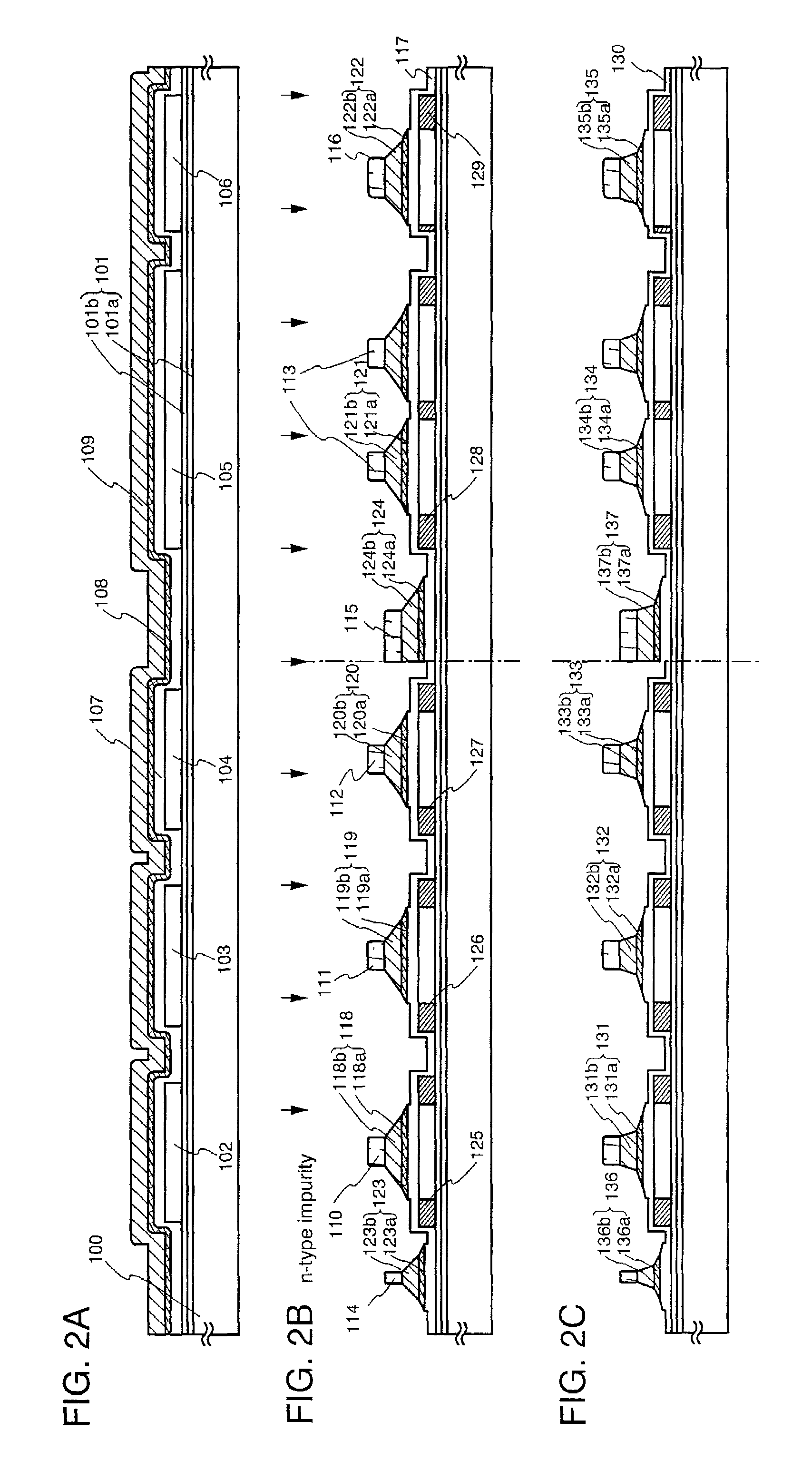
[0124]A method of manufacturing a pixel portion and TFTs (an n-channel TFT and a p-channel TFT) of a driver circuit formed in the periphery of the pixel portion, at the same time and on the same substrate is explained in detail in Embodiment 1.

[0125]First, as shown in FIG. 2A, a base film 101 made of an insulating film such as a silicon oxide film, a silicon nitride film, or a silicon oxynitride film, is formed on a substrate 100 made from a glass such as barium borosilicate glass or aluminum borosilicate glass, typically a glass such as Corning Corp. #7059 glass or #1737 glass. For example, a lamination film of a silicon oxynitride film 101a, manufactured from SiH4, NH3, and N2O by plasma CVD, and formed having a thickness of 10 to 200 nm (preferably between 50 and 100 nm), and a hydrogenated silicon oxynitride film 101b, similarly manufactured from SiH4 and N2O, and formed having a thickness of 50 to 200 nm (preferably between 100 and 150 nm), is formed. A two layer ...

embodiment 2

[Embodiment 2]

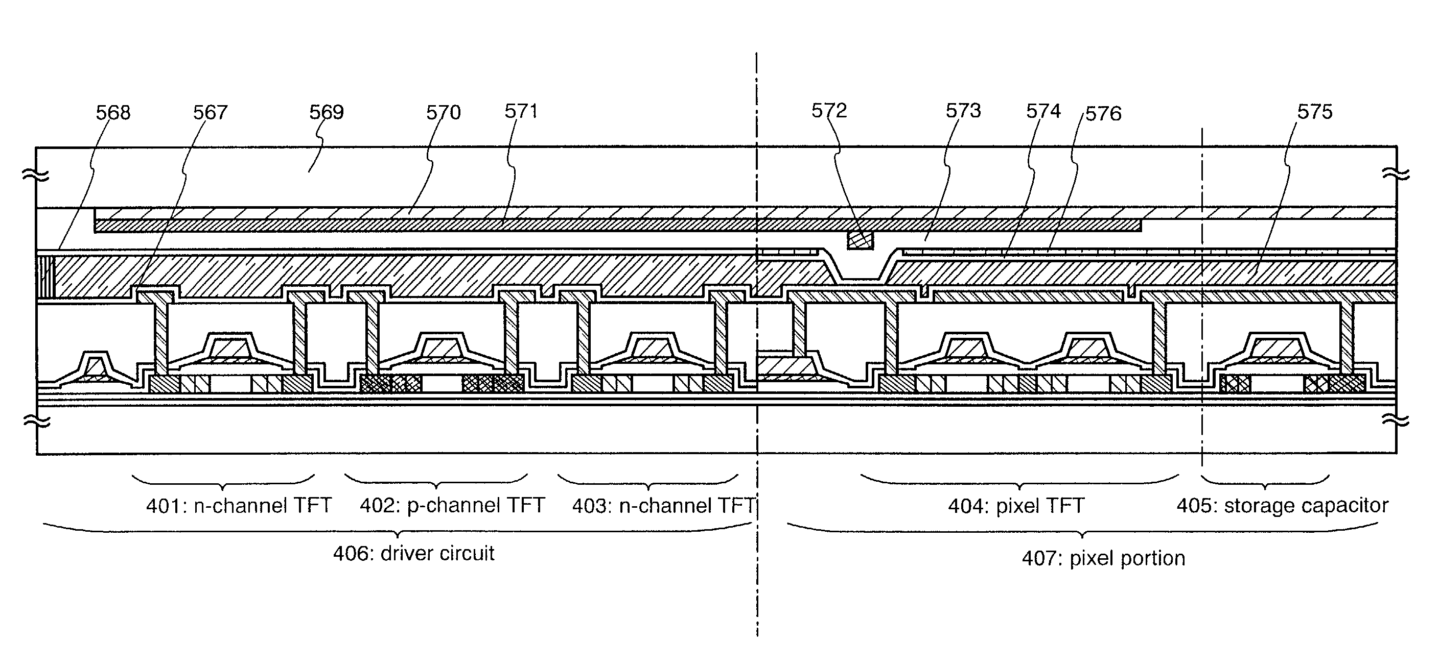
[0158]A process of manufacturing an active matrix liquid crystal display device from the active matrix substrate manufactured in Embodiment 1 is explained below in Embodiment 2. FIG. 5 is used for the explanation.

[0159]After first obtaining the active matrix substrate of FIG. 4 in accordance with Embodiment 1, an orientation film 567 is formed on the active matrix substrate of FIG. 4, and a rubbing process is performed.

[0160]An opposing substrate 569 is prepared. Color filter layers 570 and 571, and an overcoat layer 573 are formed on the opposing substrate 569. The color filter layers are formed such that the color filter layer 570, having a red color, and the color filter 571, having a blue color, are overlapped with each other, and also serve as a light shielding film. It is necessary to shield at least the spaces between the TFTs, and the connection electrodes and the pixel electrodes when using the substrate of Embodiment 1, and therefore, it is preferable that th...

embodiment 3

[Embodiment 3]

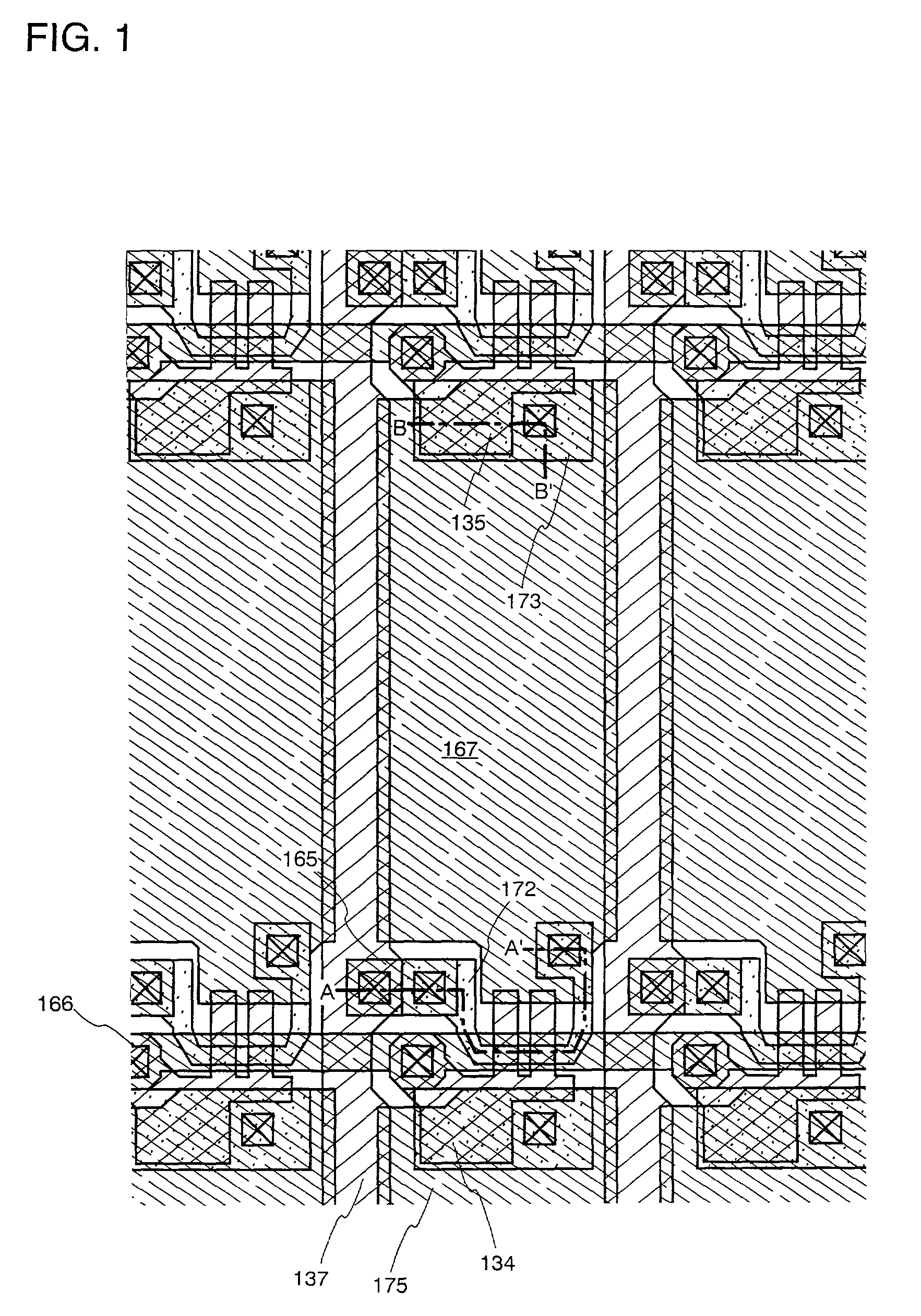
[0165]The structure of the active matrix liquid crystal display device (FIG. 5) obtained by using Embodiment 2 will be described with reference to the top view of FIG. 7A. The components corresponding to those in FIG. 5 are designated by the same reference numerals.

[0166]In the top view shown in FIG. 7A, the pixel portion, the driver circuit, an external input terminal 203 to which an FPC (Flexible Printed Circuit) is bonded, a wiring 204 for connecting the external input terminal 203 with input sections of the respective circuits, and the like are formed on an active matrix substrate 201. The active matrix substrate 201 and an opposing substrate 569, on which a color filter and the like are formed, are bonded with each other, sandwiching an end-sealing material 568 therebetween.

[0167]A light-shielding film 207 made of a red color filter or a lamination film of a red color filter and a blue color filter is formed on the upper surfaces of a gate wiring side driver circu...


PUM

PropertyMeasurementUnit
thicknessaaaaaaaaaa
thicknessaaaaaaaaaa
thicknessaaaaaaaaaa

Abstract

The present invention improves the aperture ratio of a pixel of a reflection-type display device or a reflection type display device without increasing the number of masks and without using a blackmask. A pixel electrode (167) is arranged so as to partially overlap a source wiring (137) for shielding the gap between pixels from light, and a thin film transistor is arranged so as to partially overlap a gate wiring (166) for shielding a channel region of the thin film transistor from light, thereby realizing a high pixel aperture ratio.

Description

BACKGROUND OF THE INVENTION[0001]1. Field of the Invention[0002]The present invention relates to a semiconductor device having a circuit constituted by thin film transistors (hereinafter, abbreviated as TFTs) and a method of manufacturing the same. For example, the present invention relates to an electro-optical device as is represented by a liquid crystal display panel and an electric appliance including such an electro-optical device as a component.[0003]In the specification, the term “semiconductor device” generically indicates the devices capable of functioning by taking advantage of semiconductor properties; an electro-optical devices, a semiconductor circuit and an electric appliance are all included in the semiconductor device.[0004]2. Description of the Related Art[0005]A technique for constituting a TFT by using a semiconductor thin film (having a thickness of about several nm to about several hundreds of nm) formed on a substrate having an insulating surface has lately att...

Claims


Application Information

Patent Timeline
Patent Type & Authority Patents(United States)
IPC IPC(8): H01L31/0376H01L29/04H01L29/22H01L29/227H01L31/036H01L31/20G02F1/136G02F1/1345G02F1/1362G02F1/1368G09F9/00G09F9/30H01L21/77H01L21/84H01L27/12H01L29/786H04N5/66
CPCH01L27/1248G02F1/136227H01L27/1214H01L29/78621H01L29/78627G02F1/1362H01L29/786H01L27/1288H01L27/1255H01L27/124G02F1/13454H01L29/42384H01L29/458H01L29/4908H01L29/78633H01L29/78645H01L2029/7863G02F1/136213G02F1/136G02F1/133345G02F1/133512G02F1/133514G02F1/133784G02F1/13394G02F1/134336G02F1/134363G02F1/13439G02F1/136286G02F1/1368G02F2201/123H01L21/02675H01L27/1222H01L27/1274H01L29/78675
Inventor YAMAZAKI, SHUNPEIKOYAMA, JUN
Owner SEMICON ENERGY LAB CO LTD
Why Eureka
Try Eureka