

Resin composition for encapsulating semiconductor chip and semiconductor device therewith
a semiconductor chip and resin composition technology, applied in semiconductor devices, solid-state devices, basic electric elements, etc., can solve the problems of no methods applicable to a wide range of applications, the reliability of mounted semiconductor devices is considerably less than that of devices of the related art, etc., to achieve the effect of improving curability and flowability, and improving the balance between curability and flowability
- Summary
- Abstract
- Description
- Claims
- Application Information
AI Technical Summary
Benefits of technology
Problems solved by technology
Method used
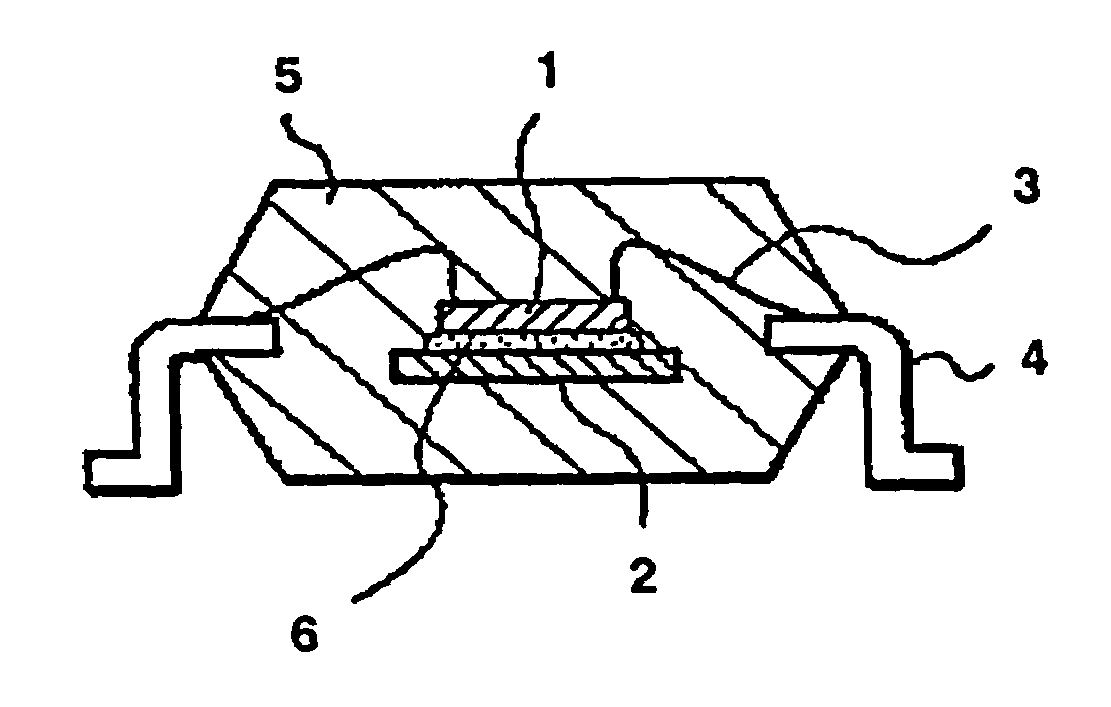
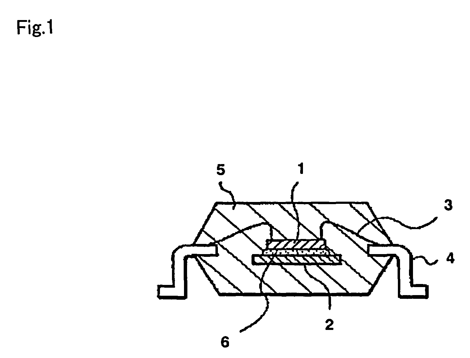
Image

Examples
example 1
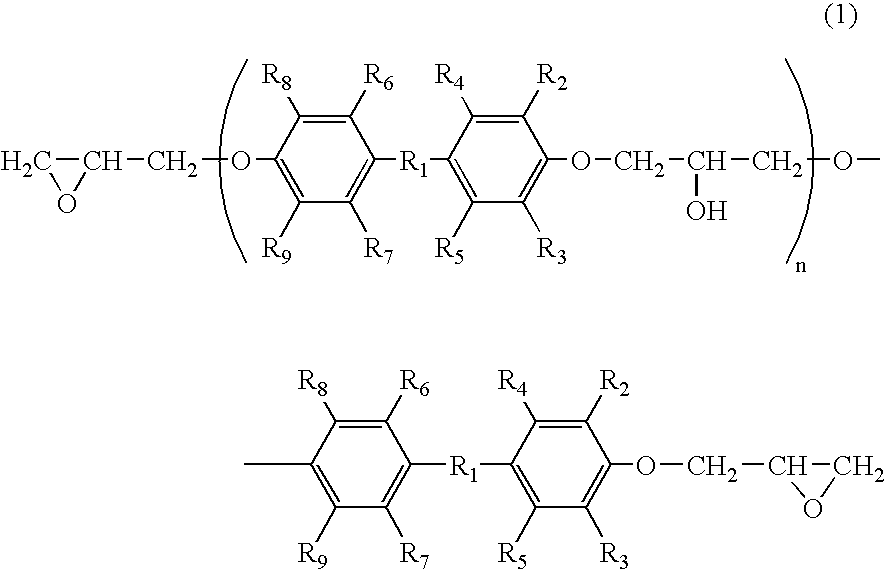
[0087]A biphenyl type epoxy resin (Japan Epoxy Resin Inc., YX4000, epoxy equivalent: 195, “n” in formula (1) is 0 (zero) as an average, melting point: 105° C.): 6.9 wt parts;
[0088]a phenolaralkyl resin (Mitsui Chemical Inc., XLC-LL, hydroxyl equivalent: 174, softening point: 79° C.): 6.05 wt parts;
[0089]spherical fused silica (average particle size: 30 μm): 86.0 wt parts;
[0090]γ-Glycidylpropyl-trimethoxysilane: 0.6 wt parts;
[0091]triphenyl phosphine: 0.2 wt parts;
[0092]2,3-dihydroxynaphthalene (Reagent grade): 0.05 wt parts;
[0093]carnauba wax: 0.2 wt parts; and
[0094]carbon black: 0.3 wt parts
[0095]were mixed in a mixer at an ambient temperature, followed by melt kneading by a heating roller at 80 to 100° C., cooling and then grinding to obtain an epoxy resin composition. The resultant epoxy resin composition was evaluated as follows. The evaluation results are shown in Table 1.
[0096]Spiral flow; the epoxy resin composition was molded by a low-pressure transfer molding machine under ...
PUM
| Property | Measurement | Unit |
|---|---|---|
| temperature | aaaaa | aaaaa |
| wt % | aaaaa | aaaaa |
| particle size | aaaaa | aaaaa |
Abstract
Description
Claims
Application Information