

Apparatus for supporting wafer in semiconductor process
a technology of apparatus and semiconductor, applied in the direction of turning machine accessories, chemical vapor deposition coating, chucks, etc., can solve the problems of complex process flow of making integrated circuits, poor uniformity of wafer edge plasma, inconsistency of wafer edge vdc, etc., to improve the improve the foregoing drawbacks, and improve the effect of etching uniformity of the wafer periphery
- Summary
- Abstract
- Description
- Claims
- Application Information
AI Technical Summary
Benefits of technology
Problems solved by technology
Method used
Image

Examples
Embodiment Construction
[0015]The preferred embodiments of the invention will now be described in greater detail. Nevertheless, it should be noted that the present invention can be practiced in a wide range of other embodiments besides those explicitly described, and the scope of the present invention is expressly not limited except as specified in the accompanying claims.
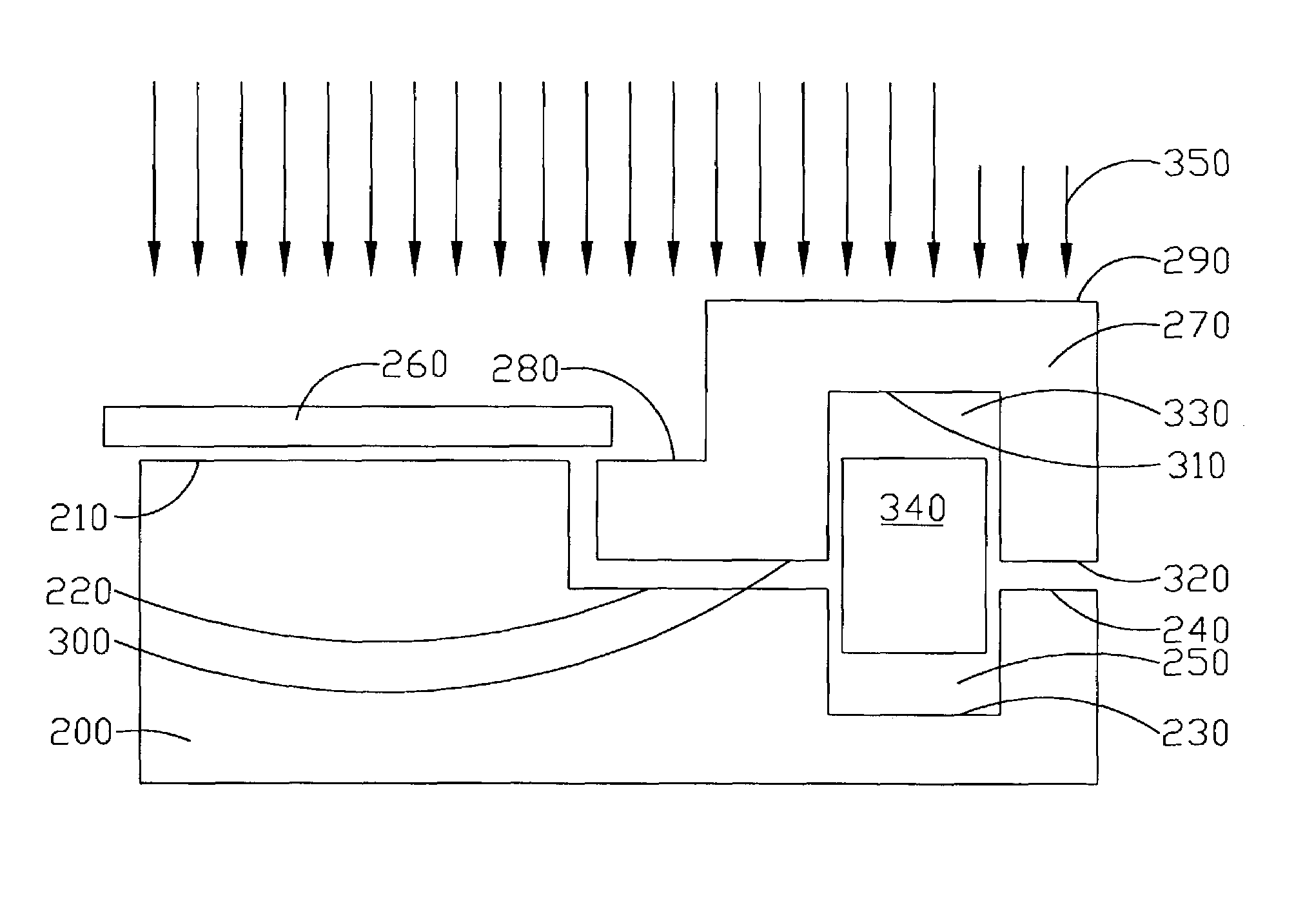
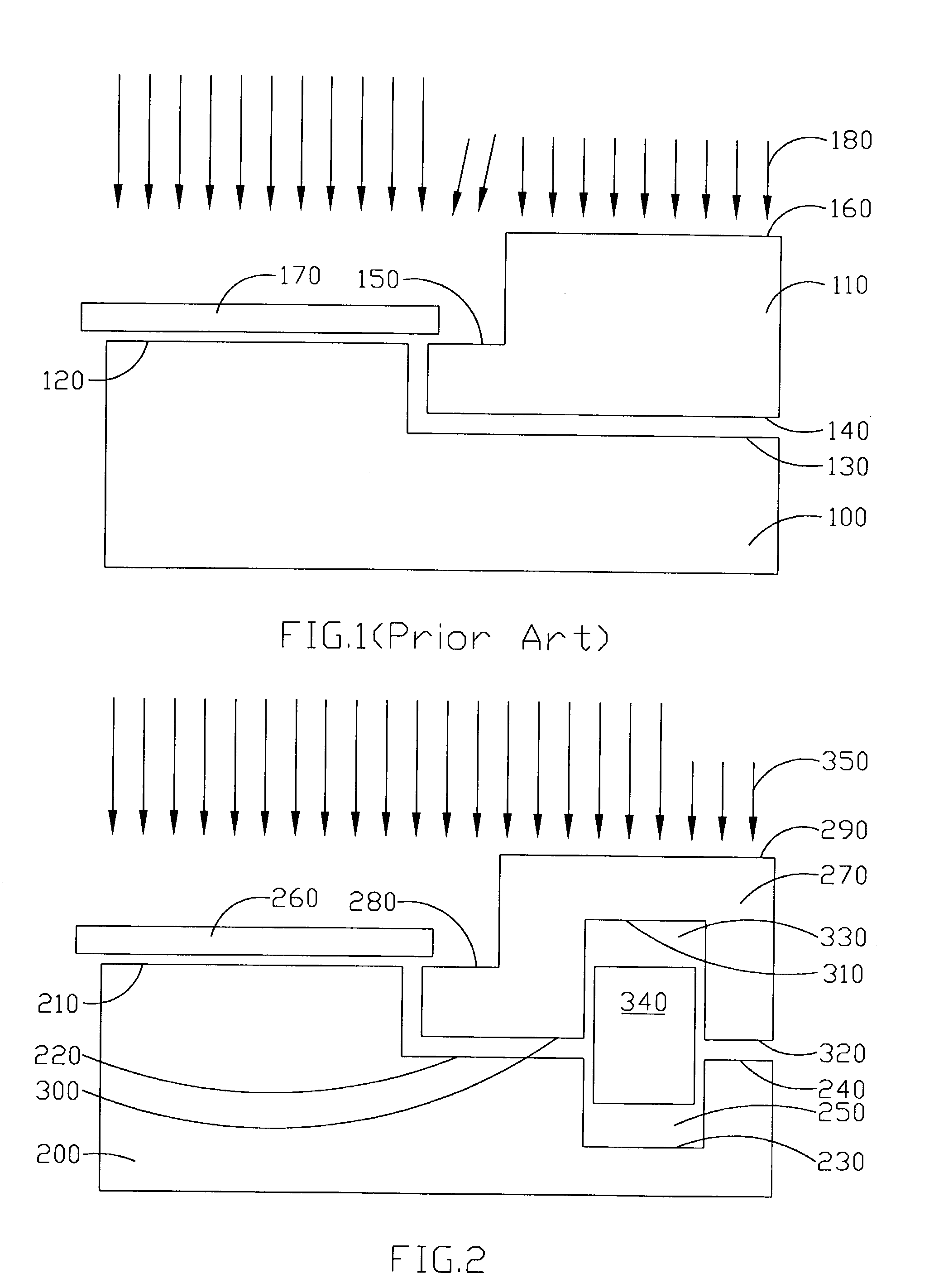
[0016]In accordance with the present invention, an apparatus for supporting a wafer in the semiconductor process, including an electrostatic chuck, a focus ring, and a conductive material. The electrostatic chuck is used in attaching a wafer during the etching process. The focus ring is used in keeping the quality of the etching uniformity of the wafer periphery. The conductive material is used in improving the etching uniformity of the wafer periphery. Herein, the conductive material is located below the focus ring of the apparatus for supporting the wafer in order to improve the plasma uniformity of the wafer periphery. By doing so, the...
PUM
| Property | Measurement | Unit |
|---|---|---|
| electromagnetic force | aaaaa | aaaaa |
| conductive | aaaaa | aaaaa |
| height | aaaaa | aaaaa |
Abstract
Description
Claims
Application Information