Multiple floating guard ring edge termination for silicon carbide devices

a technology of silicon carbide and edge termination, which is applied in the direction of semiconductor/solid-state device manufacturing, semiconductor devices, electrical devices, etc., can solve the problems of affecting the breakdown voltage of the device, affecting the switching speed of silicon-based pin devices, and requiring additional fabrication costs

Active Publication Date: 2006-04-11
CREE INC
View PDF46 Cites 126 Cited by
  • Summary
  • Abstract
  • Description
  • Claims
  • Application Information

AI Technical Summary

Problems solved by technology

Silicon-based PIN devices typically exhibit relatively poor switching speeds.
Surface effects may cause the depletion region to spread unevenly, which may adversely affect the breakdown voltage of the device.
Furthermore, additional fabrication costs may be incurred as a result of added photolithography and implantation steps.
This leads to very high oxide fields and may result in long-term reliability problems.
Thus, FP may be unsuitable for use in SiC devices.
Kinoshita et al. reported that such techniques reduced the sensitivity to implant dose variation.
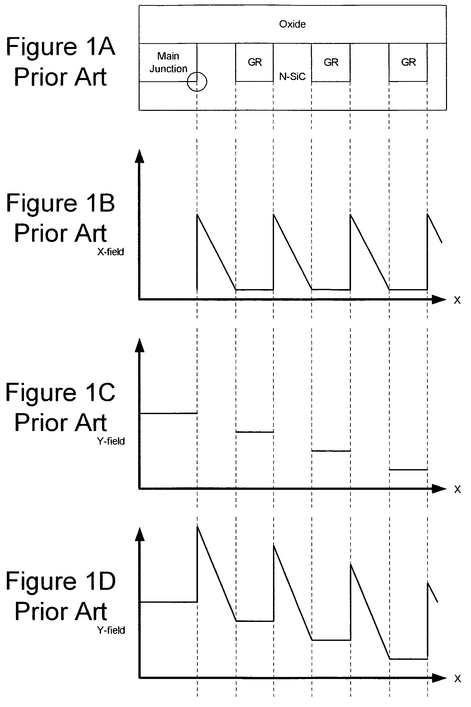
However, MFGR may be very sensitive to surface charges in the oxide-semiconductor interface.
One potentially critical issue with the MFGR termination scheme is that it is very sensitive to the charge at the oxide-semiconductor interface.
However, field oxides often typically have lower quality when compared to thermally grown gate oxides and plasma processing steps may result in higher oxide charges.
This results in very high field at the oxide-semiconductor interface and, therefore, reduces the effectiveness of the floating guard rings that may result in a reduction of blocking voltage for the devices.
In addition, this charge, mostly positive, can move towards or away from the oxide-semiconductor interface, causing time dependent breakdown voltage, or breakdown walk-out.
This problem may be even greater in silicon carbide devices because the field oxides are generally deposited.
Deposited oxides, typically, have inferior characteristics to those of thermally grown layers, and the oxide-semiconductor interface in a silicon carbide device has much greater charge density compared to that of a silicon device.
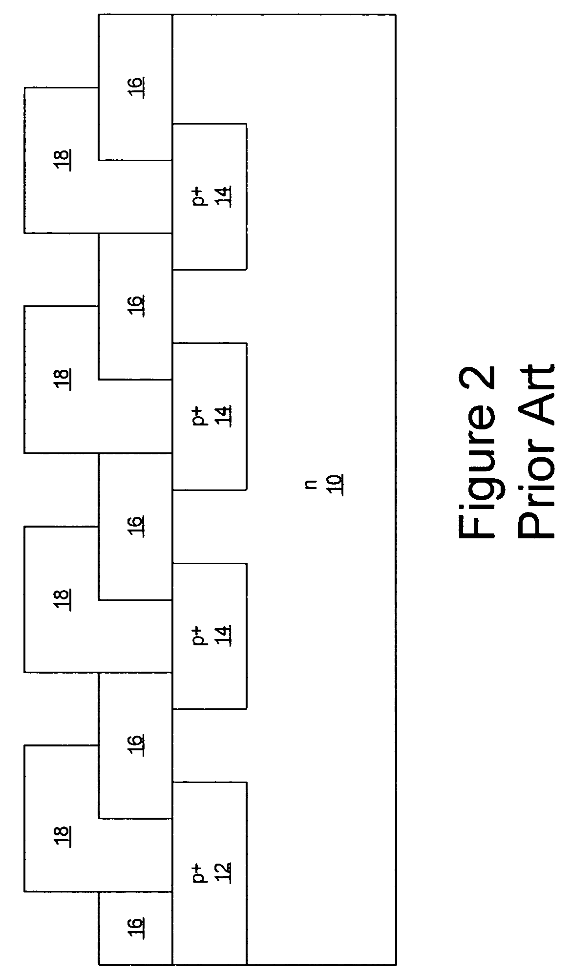
Such requirements may be difficult to achieve with conventional fabrication techniques, such as photolithography, for silicon carbide devices because the Offset Field Plate-Floating Guard Ring structure has each field plate contacting each guard ring separately and the edge of the guard ring should not overlap with the edge of the next guard ring.
Such alignment requirements may be difficult, if not impossible, to achieve with conventional contact aligners for SiC.
Step coverage may also be another issue with the Offset Field Plate-Floating Guard Ring structure because the thickness of the oxide that may be needed.
Oxides in silicon carbide devices, generally have lower quality than that available in silicon devices.
Accordingly, the Offset Field Plate-Floating Guard Ring structure may not be practical for silicon carbide devices.

Method used


Image

  • Multiple floating guard ring edge termination for silicon carbide devices
  • Multiple floating guard ring edge termination for silicon carbide devices
  • Multiple floating guard ring edge termination for silicon carbide devices

Examples


examples

[0054]The following examples are illustrative of particular embodiments of the present invention and should not be construed as limiting embodiments of the present invention.

[0055]Schottky diodes with a 1.58 mm2 active area were fabricated utilizing the junction termination techniques according to embodiments of the present invention. The various junction termination configurations are described in Table 1 below. In Table 1, the devices are identifed by the number of guard rings (GR), whether a junction termination extension (JTE) was present, and if so, where the JTE was located and if the charge compensation layer (player) was present in the device. The reference to 1-zone JTE refers to a device having a single doping level JTE. The various physical and electrical characteristics of the devices are also provided in Table 1. In Table 1, BV refers to breakdown voltage and the average (AVE) and maximum (MAX) breakdown voltage for devices on one of the six wafers fabricated are provid...


PUM

PropertyMeasurementUnit
distanceaaaaaaaaaa
distanceaaaaaaaaaa
electric fieldsaaaaaaaaaa

Abstract

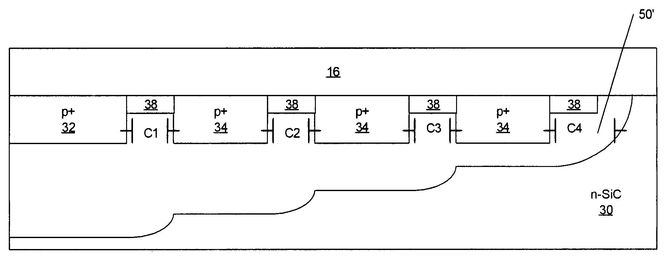
Edge termination for silicon carbide devices has a plurality of concentric floating guard rings in a silicon carbide layer that are adjacent and spaced apart from a silicon carbide-based semiconductor junction. An insulating layer, such as an oxide, is provided on the floating guard rings and a silicon carbide surface charge compensation region is provided between the floating guard rings and is adjacent the insulating layer. Methods of fabricating such edge termination are also provided.

Description

RELATED APPLICATIONS[0001]The present application claims priority from U.S. Provisional Patent Application Ser. No. 60 / 440,193, entitled “MULTIPLE FLOATING GUARD RING EDGE TERMINATION FOR SILICON CARBIDE DEVICES AND METHODS OF FABRICATING SILICON CARBIDE DEVICES INCORPORATING SAME,” and filed Jan. 15, 2003, the disclosure of which is incorporated herein by reference as if set forth fully.FIELD OF THE INVENTION[0002]The present invention relates microelectronic devices and more particularly to edge termination for silicon carbide devices.BACKGROUND OF THE INVENTION[0003]High voltage silicon carbide (SiC) Schottky diodes, which can handle voltages between, for example, about 600V and about 2.5 kV, are expected to compete with silicon PIN diodes fabricated with similar voltage ratings. Such diodes may handle as much as about 100 amps or more of current, depending on their active area. High voltage Schottky diodes have a number of important applications, particularly in the field of pow...

Claims


Application Information

Patent Timeline
Patent Type & Authority Patents(United States)
IPC IPC(8): H01L31/0312H01L29/06H01L29/24
CPCH01L29/1608H01L29/0619H01L29/872H01L29/06
Inventor RYU, SEI-HYUNGAGARWAL, ANANT K.
Owner CREE INC
Why Eureka
Try Eureka