Semiconductor package for three-dimensional mounting, fabrication method thereof, and semiconductor device

a semiconductor and three-dimensional mounting technology, applied in the direction of printed circuit assembling, printed circuit manufacturing, basic electric elements, etc., can solve the problems of high cost of mother boards, inability to stack, and limited packaging density of semiconductor packages, and achieve the effect of easy fabrication and high packaging density

Inactive Publication Date: 2006-04-18
LAPIS SEMICON CO LTD
View PDF9 Cites 43 Cited by
  • Summary
  • Abstract
  • Description
  • Claims
  • Application Information

AI Technical Summary

Benefits of technology

[0025]As described above, according to the present invention, elements can be mounted on a mother board in a three-dimensional manner. Therefore, there is provided a semiconductor package for three-dimensional mounting which can be mounted at a higher packaging density than conventional ...

Problems solved by technology

However, the BGA type semiconductor packages are mounted onto a mother board only in a two-dimensional manner and cannot be stacked.
Thus, there are limitation...

Method used


Image

  • Semiconductor package for three-dimensional mounting, fabrication method thereof, and semiconductor device
  • Semiconductor package for three-dimensional mounting, fabrication method thereof, and semiconductor device
  • Semiconductor package for three-dimensional mounting, fabrication method thereof, and semiconductor device

Examples


first embodiment

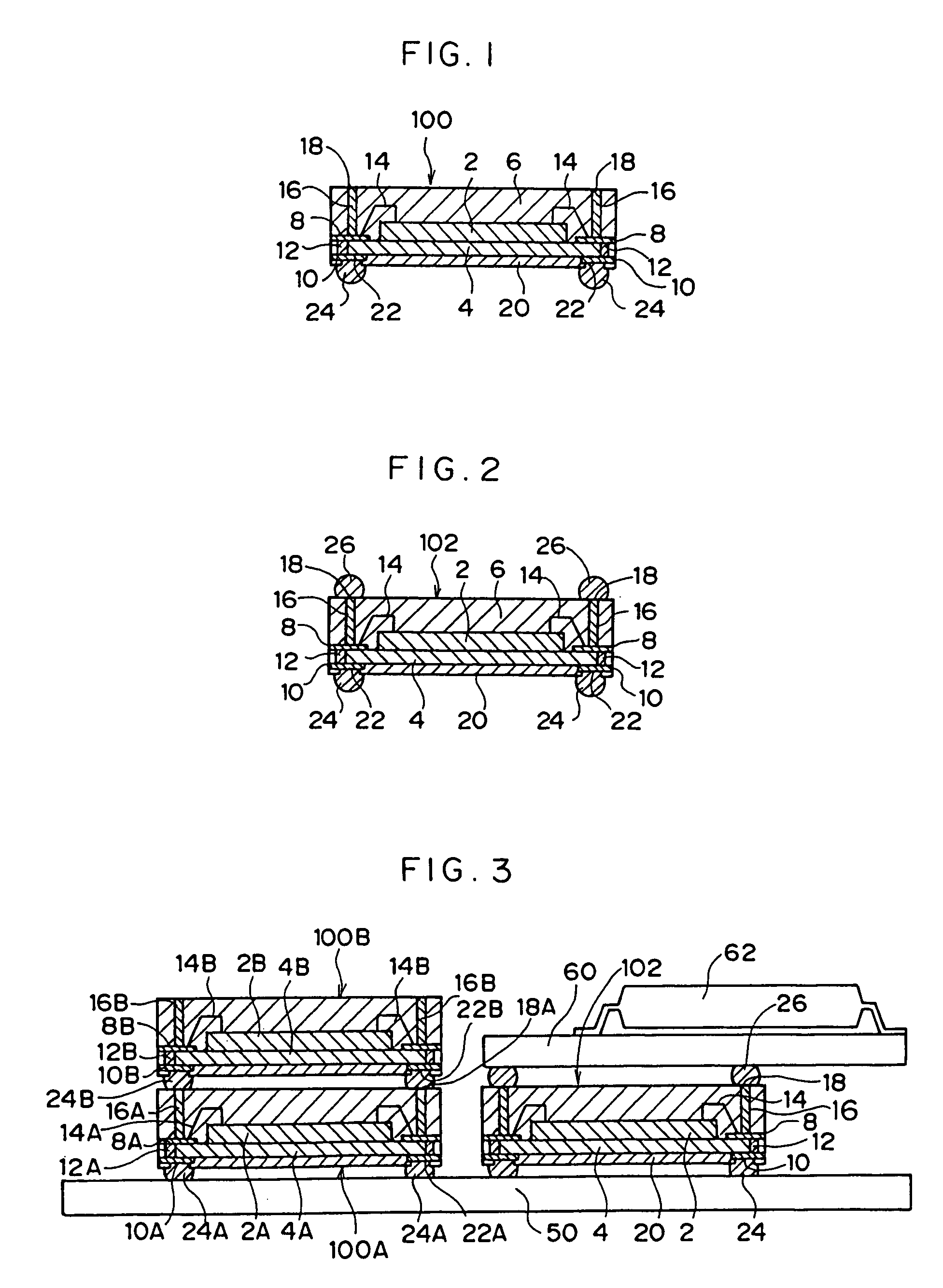
[0041]An example of a semiconductor package for three-dimensional mounting according to the present invention is shown in FIGS. 1 and 2.

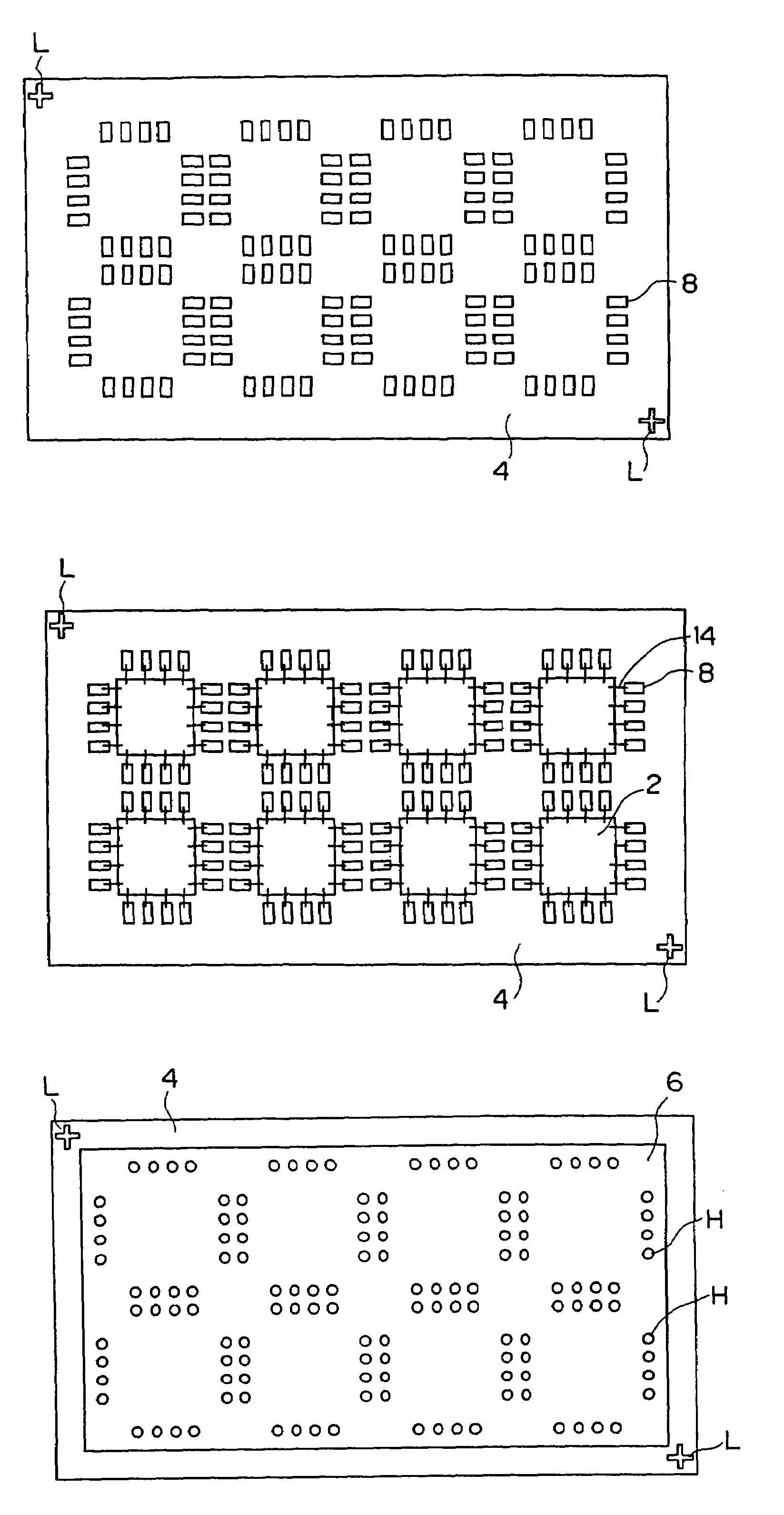
[0042]As illustrated in FIG. 1, a semiconductor package 100 for three-dimensional mounting according to the first embodiment includes a wiring substrate 4 and a semiconductor chip 2 placed on one surface of the wiring substrate 4.

[0043]A first pattern (or, upper pattern) 8 is formed at the surface of the wiring substrate 4 on which the semiconductor chip 2 is placed, while a second pattern (or, lower pattern) 10 is formed at a surface of the wiring substrate 4 opposite the first pattern 8. The first wiring pattern 8 and the second wiring pattern 10 are connected to each other via through holes 12 which pass through the wiring substrate 4.

[0044]The surface of the wiring substrate 4 having the second wiring pattern 10 formed thereon is covered with a resist layer 20 which is formed by a photoresist resin. Openings 22, which are each circular and serve...

second embodiment

[0078]Another example of the semiconductor package for three-dimensional mounting according to the present invention is shown in FIGS. 10 and 11. In these figures, reference numerals which are the same as those shown in FIGS. 1 to 3 indicate components identical to those indicated by the reference numerals in FIGS. 1 to 3.

[0079]As illustrated in FIG. 10, a semiconductor package 104 for three-dimensional mounting according to the second embodiment has a structure in which a rewiring substrate 30 is placed, via the solder balls 26, on the upper connecting surfaces 18 of the semiconductor package for three-dimensional mounting according to the first embodiment, which upper connecting surfaces 18 are located at one end of the thickness direction wires 16.

[0080]A third wiring pattern 32, which may be different from the first wiring pattern 8 and the second wiring pattern 10, is formed at an upper surface of the rewiring substrate 30. The third wiring pattern 32 is electrically connected ...

third embodiment

[0084]Still another example of the semiconductor package for three-dimensional mounting according to the present invention is illustrated in FIGS. 12A and 12B. FIG. 12A shows a cross-section of a semiconductor package for three-dimensional mounting in a thickness direction, while FIG. 12B shows the shape of the semiconductor package for three-dimensional mounting when seen from the top. Reference numerals which are the same as those in FIGS. 1 to 3 indicate components identical to those indicated by the reference numerals in FIGS. 1 to 3.

[0085]As shown in FIGS. 12A and 12B, a semiconductor package 106 for three-dimensional mounting according to the third embodiment has a structure in which a fourth wiring pattern 40 is formed at the upper surface of the sealing resin layer 6 of the semiconductor package for three-dimensional mounting according to the first embodiment. Further, the fourth wiring pattern 40 is electrically connected to the connecting surfaces 18 of the semiconductor p...


PUM


Abstract

A semiconductor package for three-dimensional mounting is provided. The package includes a wiring substrate having a first surface on which a first wiring pattern is formed and a second surface on which a second wiring pattern is formed, the first wiring pattern and second wiring pattern being electrically connected to each other; a semiconductor chip placed on the first surface of the wiring substrate and electrically connected to the first wiring pattern; a sealing resin layer sealing the semiconductor chip and the first wiring pattern; a thickness direction wire passing through the sealing resin layer in a thickness direction and having one end electrically connected to the first wiring pattern and the other end exposed at the surface of the sealing resin layer; and a lower surface connecting electrode formed on the second surface of the wiring substrate and electrically connected to the second wiring pattern.

Description

[0001]This is a Divisional of U.S. application Ser. No. 09 / 942,962, filed Aug. 31, 2001 now U.S. Pat. No. 6,740,964, the subject matter of which is incorporated herein by reference.BACKGROUND OF THE INVENTION[0002]1. Field of the Invention[0003]The present invention relates to a semiconductor package for three-dimensional mounting, a fabrication method thereof, and a semiconductor device. More specifically, the present invention relates to a semiconductor package for three-dimensional mounting which is easy to fabricate and has high packaging density, a fabrication method thereof, and a semiconductor device in which the semiconductor package for three-dimensional mounting is mounted onto a mother board.[0004]2. Description of the Related Art[0005]An example of a conventional BGA (i.e., ball grid array) type semiconductor package is illustrated in FIG. 15.[0006]As illustrated in FIG. 15, a conventional BGA type semiconductor package includes a wiring substrate B and a semiconductor c...

Claims


Application Information

Patent Timeline
IPC IPC(8): H01L21/44H01L23/28H01L21/56H01L23/12H01L23/31H01L23/52H01L25/065H05K1/14H05K3/34
CPCH01L23/3128H01L25/105H01L24/97H01L2225/1058H01L2223/5442H01L2223/54473H01L2224/48095H01L2224/48227H01L2224/49175H01L2224/97H01L2924/01004H01L2924/01029H01L2924/01047H01L2924/01078H01L2924/01079H01L2924/15311H05K1/145H05K3/3436H01L2225/1041H01L2225/1023H01L24/49H01L2924/19107H01L2924/01033H01L2924/01006H01L2924/01005H01L2225/1052H01L24/48H01L2224/85H01L2924/00014H01L2924/00H01L2924/12042H01L2924/181H01L24/45H01L2224/05599H01L2224/45139H01L2224/45144H01L2224/85399H01L2924/00012H01L2224/45015H01L2924/207H01L21/44H01L23/28
Inventor SASAKI, TAKAAKI
Owner LAPIS SEMICON CO LTD
Why Eureka
Try Eureka