Photovoltaic device with intrinsic amorphous film at junction, having varied optical band gap through thickness thereof

Inactive Publication Date: 2006-04-18
SANYO ELECTRIC CO LTD
View PDF33 Cites 69 Cited by
  • Summary
  • Abstract
  • Description
  • Claims
  • Application Information

AI Technical Summary

Benefits of technology

[0019]In other words, the intrinsic amorphous semiconductor layer of high quality is provided on the crystalline semiconductor substrate side, while the intrinsic amorphous semiconductor layer having a large optical band gap, that is, a wide gap is provided on the amorphous semiconductor film side. By providing the intrinsic

Problems solved by technology

However, since the thin film semiconductor has a disordered crystalline structure, it has a large number of unbonded sites or ends on a crystalline structure and is not

Method used


Image

  • Photovoltaic device with intrinsic amorphous film at junction, having varied optical band gap through thickness thereof
  • Photovoltaic device with intrinsic amorphous film at junction, having varied optical band gap through thickness thereof
  • Photovoltaic device with intrinsic amorphous film at junction, having varied optical band gap through thickness thereof

Examples


first embodiment

(First Embodiment)

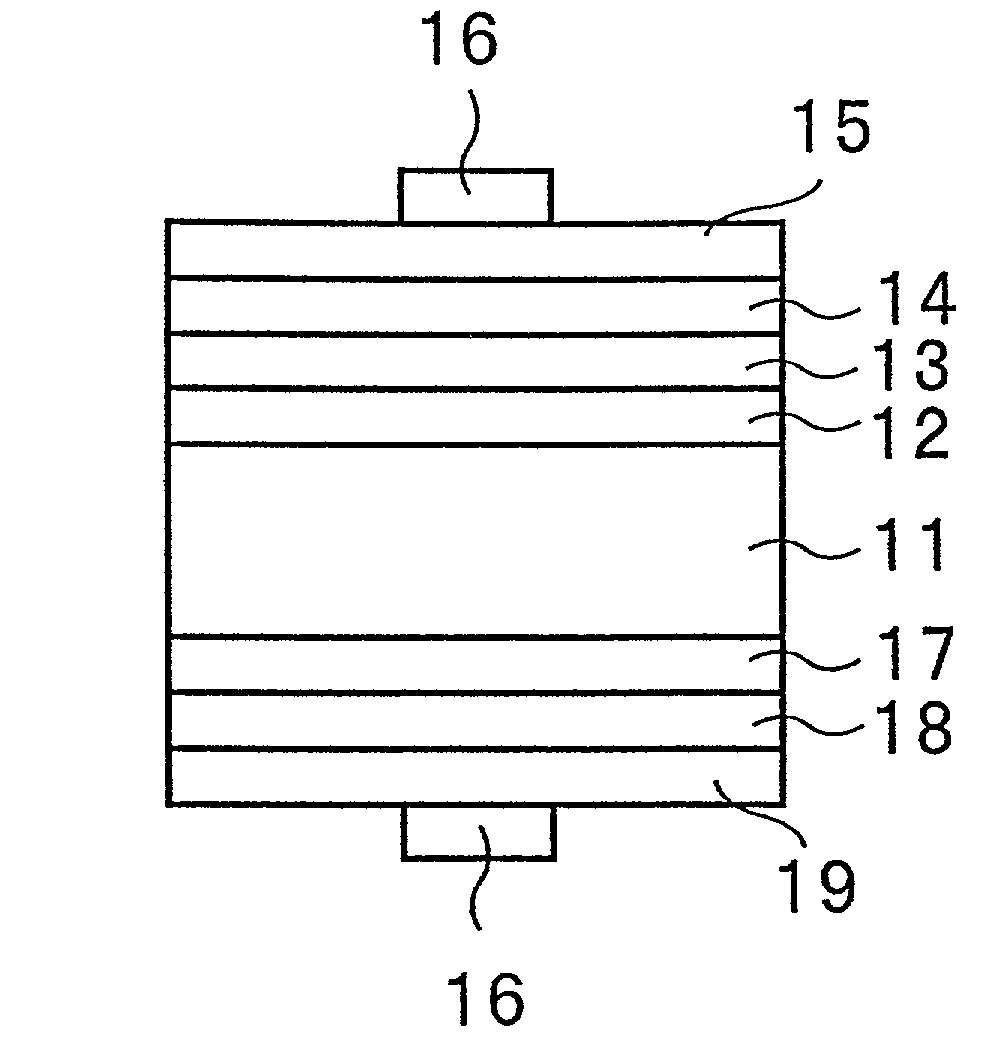
[0030]FIG. 1 is a typical sectional view showing a photovoltaic device according to a first embodiment of the present invention. With reference to FIG. 1, an intrinsic amorphous silicon layer 12 is formed on the light incidence side of an n-type single crystalline silicon substrate 11. An intrinsic amorphous silicon carbide layer 13 is formed on the intrinsic amorphous silicon layer 12. The intrinsic amorphous semiconductor film according to the present invention is constituted by the intrinsic amorphous silicon layer 12 and the intrinsic amorphous silicon carbide layer 13. Ap-type amorphous silicon film 14 is formed on the intrinsic amorphous silicon carbide layer 13. A transparent electrode 15 is formed on the p-type amorphous silicon film 14 and a collector electrode 16 is provided on the transparent electrode 15.

[0031]An intrinsic amorphous silicon layer 17 is formed on the back face side of the n-type single crystalline silicon substrate 11 and an n-type amorp...

second embodiment

(Second Embodiment)

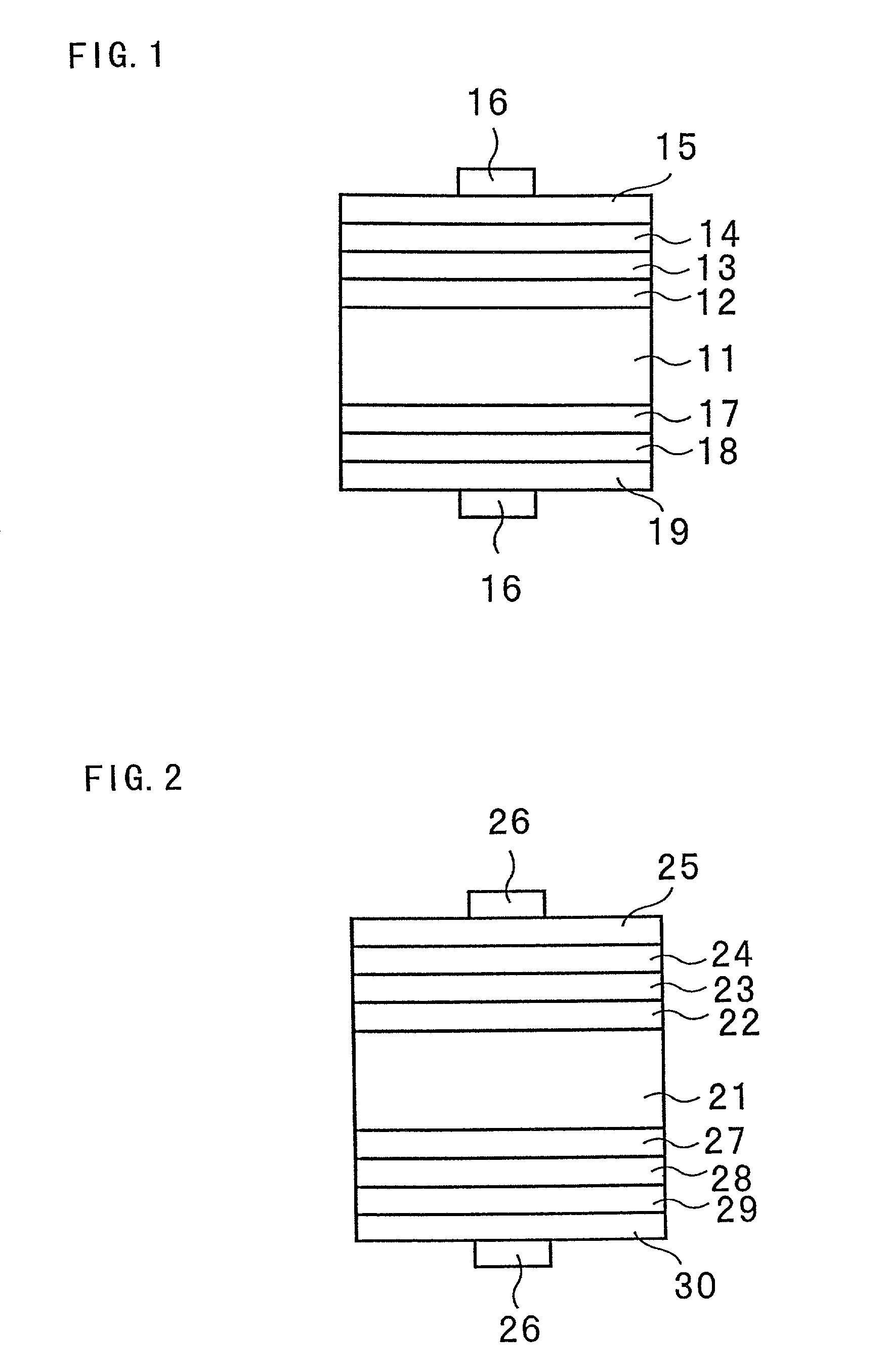
[0047]FIG. 2 is a typical sectional view showing a photovoltaic device according to a second embodiment of the present invention.

[0048]With reference to FIG. 2, an intrinsic amorphous silicon layer 22 is formed on the light incidence side of an n-type single crystalline silicon substrate 21 and an intrinsic amorphous silicon carbide layer 23 is formed on the intrinsic amorphous silicon layer 22. The intrinsic amorphous semiconductor film according to the present invention is constituted by the intrinsic amorphous silicon layer 22 and the intrinsic amorphous silicon carbide layer 23. A p-type amorphous silicon film24 is formed on the intrinsic amorphous silicon carbide layer 23, and a transparent electrode 25 and a collector electrode 26 are formed on the p-type amorphous silicon film 24.

[0049]An intrinsic amorphous silicon layer 27 is formed on the back face side of the n-type single crystalline silicon substrate 21 and an intrinsic amorphous silicon carbide layer...

third embodiment

(Third Embodiment)

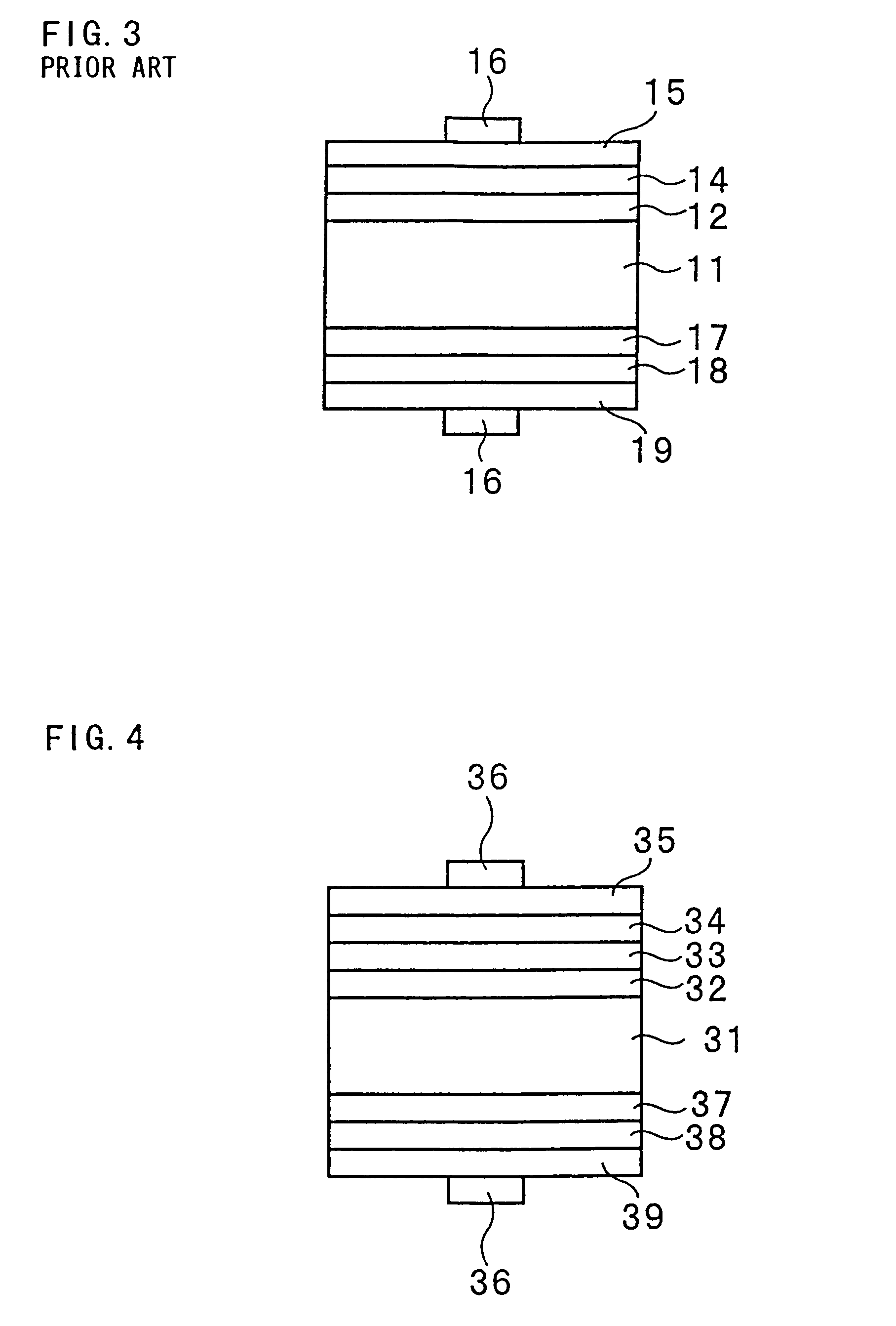
[0058]FIG. 4 is a typical sectional view showing a photovoltaic device according to a third embodiment of the present invention. With reference to FIG. 4, an intrinsic amorphous silicon layer 32 is formed on the light incidence side of an n-type single crystalline silicon substrate 31 and an intrinsic amorphous silicon layer 33 is formed on the intrinsic amorphous silicon layer 32. The intrinsic amorphous silicon layer 33 is formed to have a relatively larger amount of hydrogen to be contained than the intrinsic amorphous silicon layer 32. More specifically, the intrinsic amorphous silicon layer 33 is formed to have an optical band gap expanded with an increase in the amount of hydrogen to be contained. An intrinsic amorphous semiconductor film according to the present invention is constituted by the intrinsic amorphous silicon layer 32 and the intrinsic amorphous silicon layer 33.

[0059]A p-type amorphous silicon layer 34 is formed on the intrinsic amorphous silico...


PUM


Abstract

In a photovoltaic device comprising a thin intrinsic amorphous semiconductor film inserted in a junction portion of a crystalline semiconductor substrate and an amorphous semiconductor film which have conductive types reverse to each other, an optical band gap of the intrinsic amorphous semiconductor film is expanded on a side in contact with the amorphous semiconductor film.

Description

BACKGROUND OF THE INVENTION[0001]1. Field of the Invention[0002]The present invention relates to a photovoltaic device, and more particularly to a photovoltaic device comprising a semiconductor junction of a crystalline semiconductor such as a single crystalline semiconductor or a polycrystalline semiconductor and an amorphous semiconductor.[0003]2. Related Art[0004]In recent years, there has vigorously been developed a photovoltaic device using a thin film semiconductor. The area of a photovoltaic device using a thin film semiconductor as a power generating layer can easily be increased and the basic requirements for the photovoltaic device such as a solar cell can be satisfied sufficiently.[0005]However, since the thin film semiconductor has a disordered crystalline structure, it has a large number of unbonded sites or ends on a crystalline structure and is not a good material as compared with the crystalline semiconductor. For this reason, there is a problem in that a high photoe...

Claims


Application Information

Patent Timeline
IPC IPC(8): H01L27/15H01L31/12H01L33/00H01L31/04H01L31/06H01L31/065H01L31/072H01L31/0745H01L31/0747H01L31/075H01L31/20
CPCH01L31/0745H01L31/0747H01L31/202Y02E10/547Y02E10/548Y02P70/50
Inventor NAKAMURA, NOBORUTAGUCHI, MIKIOKAWAMOTO, KUNIHIRO
Owner SANYO ELECTRIC CO LTD
Why Eureka
Try Eureka