Eureka AIR delivers breakthrough ideas for toughest innovation challenges, trusted by R&D personnel around the world.

Suspended and truncated co-planar waveguide

Active Publication Date: 2006-04-25
OPLINK COMM
View PDF1 Cites 4 Cited by
  • Summary
  • Abstract
  • Description
  • Claims
  • Application Information

AI Technical Summary

Problems solved by technology

However, the major drawback with microstrip line is the difficulty encountered in placing series and shunt components on the same surface as the microstrip signal conductor.
The problem arises because the ground conductor—to which electrical contact is essential for the operation of many components—is conventionally formed on the backside of a substrate (e.g. Duroid, ceramic, etc.) on which the microstrip line is formed.
The conducting material used in the via holes adds parasitics, such as unwanted inductances and resistances, to circuits assembled on the top side of the substrate.
The parasitics in many cases lead to limits on the high frequency performance of the microstrip lines and circuits that include them.
However, such a structure is impractical to construct.
The disadvantages of CPWs include the higher possibility of dominant undesired mode generation and lower power handling capability as compared to other available transmission media in the frequency bands of interest.
There is especially a problem with spurious mode (i.e. unwanted electromagnetic wave modes) generation associated with broadband signal transmission on Conductor-Backed Coplanar Waveguides (CBCPW).
Unfortunately, currently known CPW structures do not provide much freedom of design that can be taken advantage of to significantly lower the effects of ISI.
Compared to the generation and characterization of picosecond electrical pulses, which is an almost fully matured technology, the development of transmission structures capable of handling the extremely wide bandwidth of these pulses still remains difficult.

Method used


Image

  • Suspended and truncated co-planar waveguide
  • Suspended and truncated co-planar waveguide
  • Suspended and truncated co-planar waveguide

Examples


Embodiment Construction

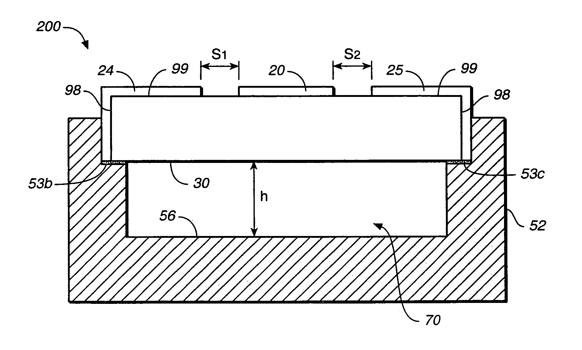
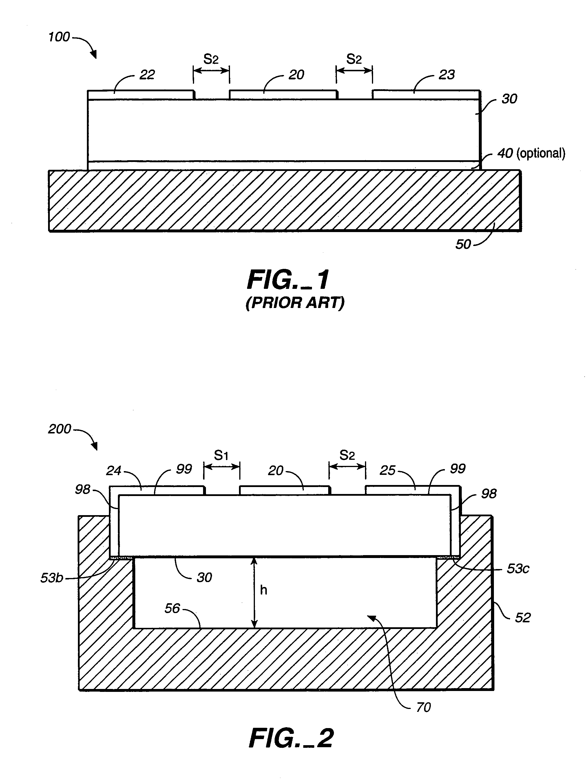
[0029]FIG. 2 shows a CPW structure 200 that includes a substrate 30 and a signal conductor 20. The CPW structure 200 has ground conductors 24 and 25 that wrap around from a top surface 99 of the substrate 30 onto the lateral faces 98 of the substrate 30. Having the ground conductors 24 and 25 extend around and over the lateral faces of the substrate provides the CPW structure 200 with an electrical side-wall boundary that acts to mitigate the effects of spurious mode generation. Suppression of spurious modes will be discussed in greater detail below.

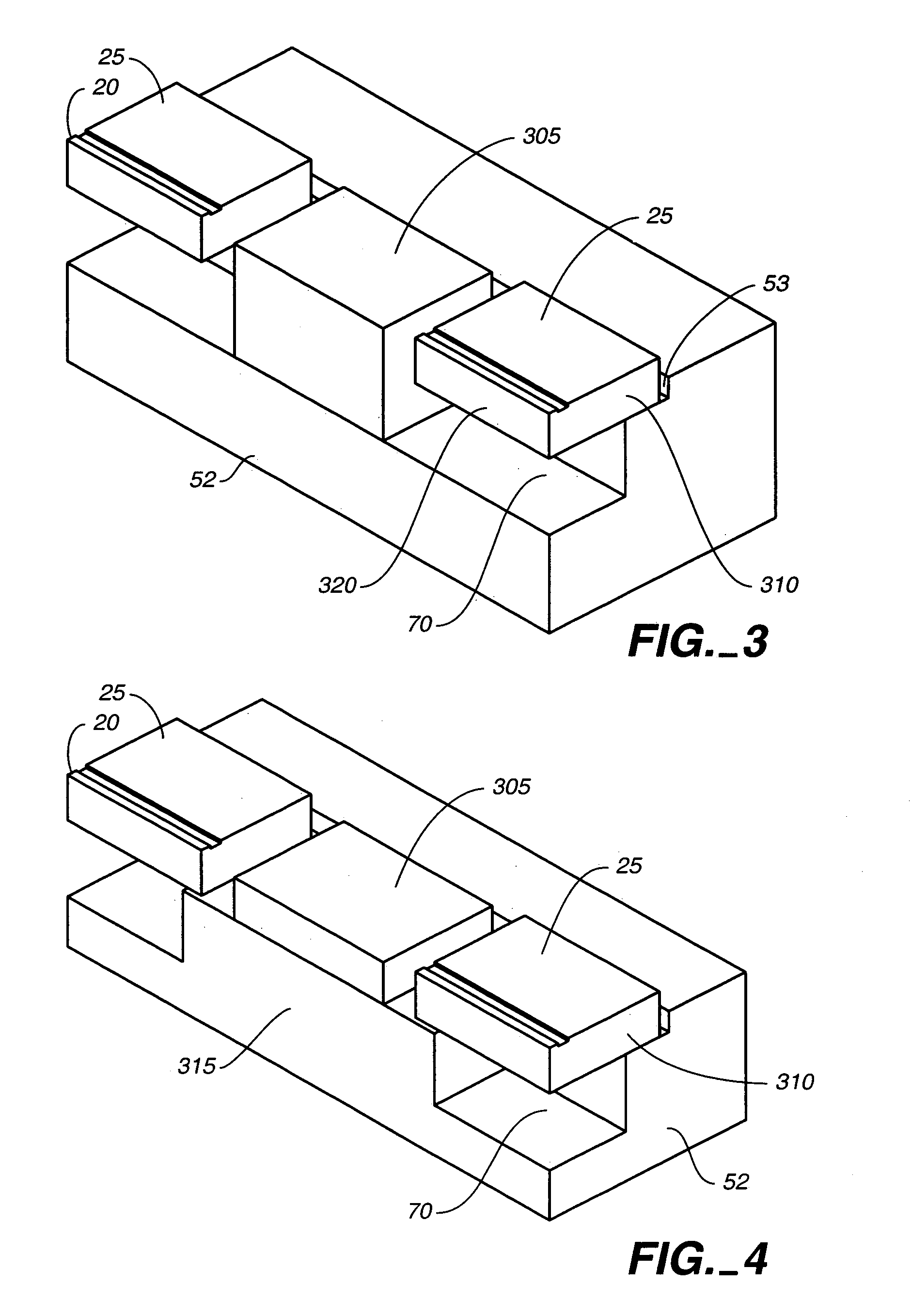
[0030]In alternative embodiments, the lateral faces 98 of the ground conductors 24 and 25 that cover the lateral faces 98 of the substrate 30 could be replaced with electrically equivalent structures. For example, grounded castellated conductive bands (not shown) that extend along the length of the lateral faces 98 of the substrate 30 could be used to provide the electrical side-wall boundary effect. Alternatively, grounded laterally spa...


PUM


Abstract

A suspended and truncated co-planar waveguide is described. The waveguide has a substrate with a substantially flat top surface and two lateral faces. A signal conductor and two ground conductors are placed on the top surface forming a ground-signal-ground pattern along a common plane. The waveguide has respective electrical side-wall boundaries on each of the two lateral faces of the substrate.

Description

[0001]This application claims the benefit of Provisional Application No. 60 / 446,258, filed Feb. 11, 2003.TECHNICAL FIELD[0002]The present invention relates generally to electrical components.BACKGROUND[0003]Until the advent of Coplanar Waveguides (CPWs), microstrip line was the conventional broadband transmission medium employed for use in electronics operating at the microwave and millimeter wave frequency bands. However, the major drawback with microstrip line is the difficulty encountered in placing series and shunt components on the same surface as the microstrip signal conductor. The problem arises because the ground conductor—to which electrical contact is essential for the operation of many components—is conventionally formed on the backside of a substrate (e.g. Duroid, ceramic, etc.) on which the microstrip line is formed. Consequently, conductor-filled via holes through the substrate must be made to connect components on the topside of the substrate with the ground conducto...

Claims


Application Information

Patent Timeline
IPC IPC(8): H01P3/08H01P3/00
CPCH01P3/003
Inventor NGUYEN, JOHN A.GUNDAVAJHALA, ANAND
Owner OPLINK COMM
Why Eureka
Eureka Blog
Learn More