Semiconductor device and method for manufacturing the same

a semiconductor device and manufacturing method technology, applied in non-linear optics, instruments, optics, etc., can solve the problems of low reliability, low yield, and difficulty in ensuring the adhesiveness of the underlying layer, so as to improve the adhesiveness, high yield, and high reliability

Inactive Publication Date: 2006-05-02
SEMICON ENERGY LAB CO LTD
View PDF9 Cites 14 Cited by
  • Summary
  • Abstract
  • Description
  • Claims
  • Application Information

AI Technical Summary

Benefits of technology

[0007]It is an object of the present invention to improve the adhesiveness between thin films, particularly the adhesiveness of an organic insulating film to be formed on an insulating surface. The present invention provides a semiconductor device with high reliability and a method for manufacturing the semiconductor device with a high yield.

Problems solved by technology

However, when an organic insulating film is used for a planarization film, adhesiveness with an underlying layer film to be laminated becomes a problem depending on a combination of materials.
In the case of poor adhesiveness, film peeling is caused.
Such the semiconductor device has a low reliability and is manufactured with a lower yield.

Method used


Image

  • Semiconductor device and method for manufacturing the same
  • Semiconductor device and method for manufacturing the same
  • Semiconductor device and method for manufacturing the same

Examples


embodiment

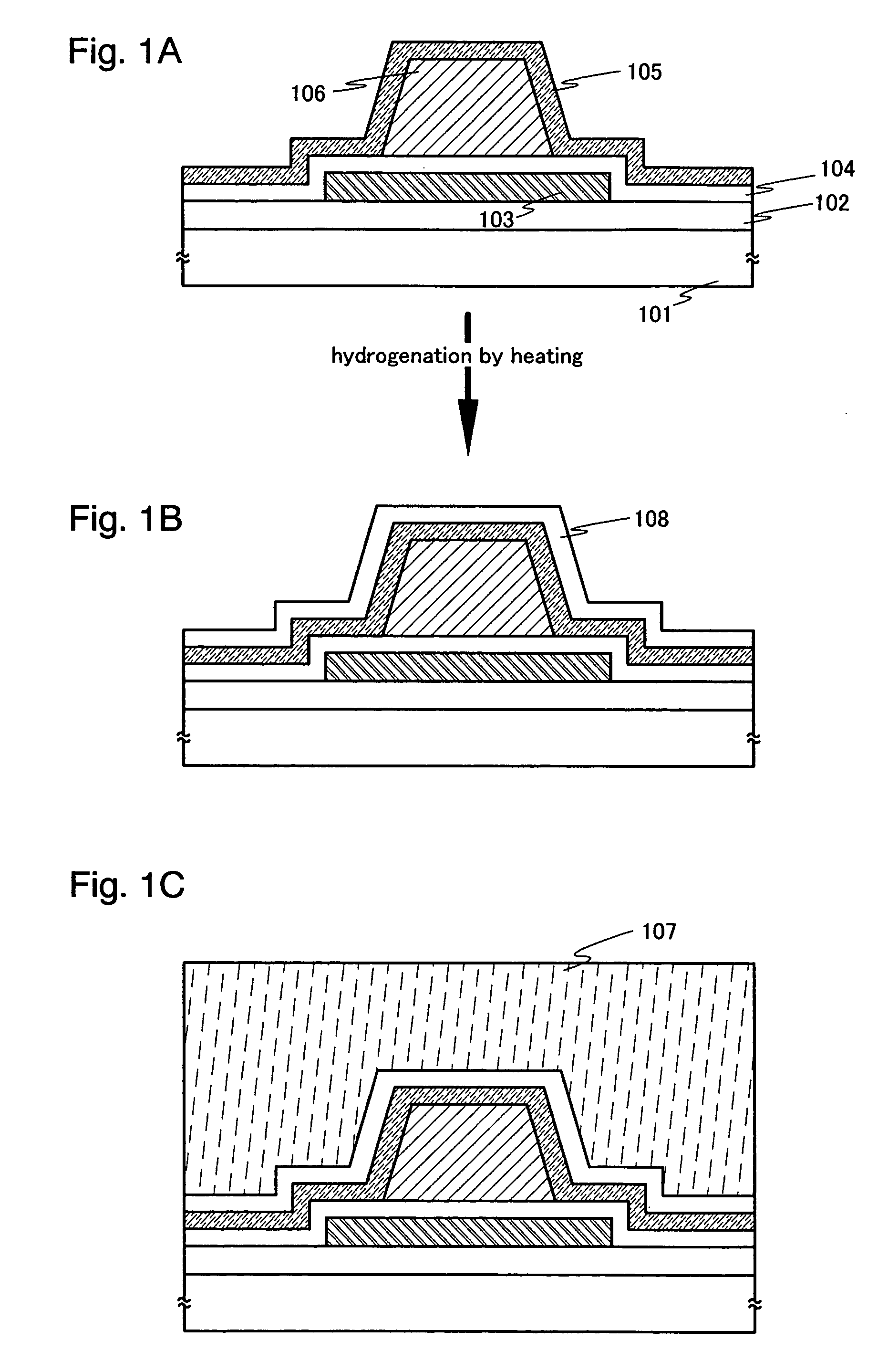
[0036]Although the present invention has been fully described by way of example with reference to the accompanying drawings, it is to be understood that various changes and modifications will be apparent to those skilled in the art. Therefore, unless otherwise such changes and modifications depart from the scope of the present invention hereinafter defined, they should be construed as being included therein. Note that, in a structure of the present invention to be described hereinafter, the same reference numbers are used for devices or portions that have the same function. Descriptions about the same reference numbers are omitted.

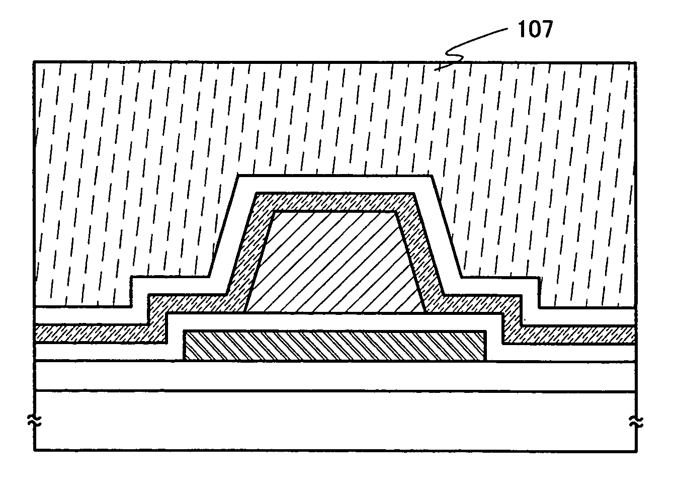
[0037]The present invention is shown in FIGS. 1A to 1C. As shown in FIG. 1A, a base film 102 is formed on a substrate 101, and a semiconductor film 103 is formed on the base film 102. For the substrate 101 over which the semiconductor film 103 is formed, a glass substrate, a quartz substrate, a plastic substrate, a metal substrate, a flexible substrate, or...

example 1

[0057]In this example, focusing attention on a property of materials of an organic insulating film and a base film in contact with a bottom surface of the organic insulating film, particularly on wettability, a relationship between the property and the adhesiveness was derived from an experiment.

[0058]In this example, two types of samples were created by forming a silicon nitride film (SiN) and a silicon nitride oxide film (SiNO) on each substrate as base films. As the substrate, a substrate with an insulating film formed on a surface of a glass substrate, a quartz substrate, a silicon substrate, a metal substrate, or a stainless substrate may be used. In this example, the glass substrate was used.

[0059]In this example, the silicon nitride film (SiN) was formed to be 100 nm in thickness on the glass substrate by plasma CVD (SiN original sample). In addition, the silicon nitride oxide film (SiNO) was also formed to be 100 nm in thickness on the glass substrate by plasma CVD (SiNO ori...

example 2

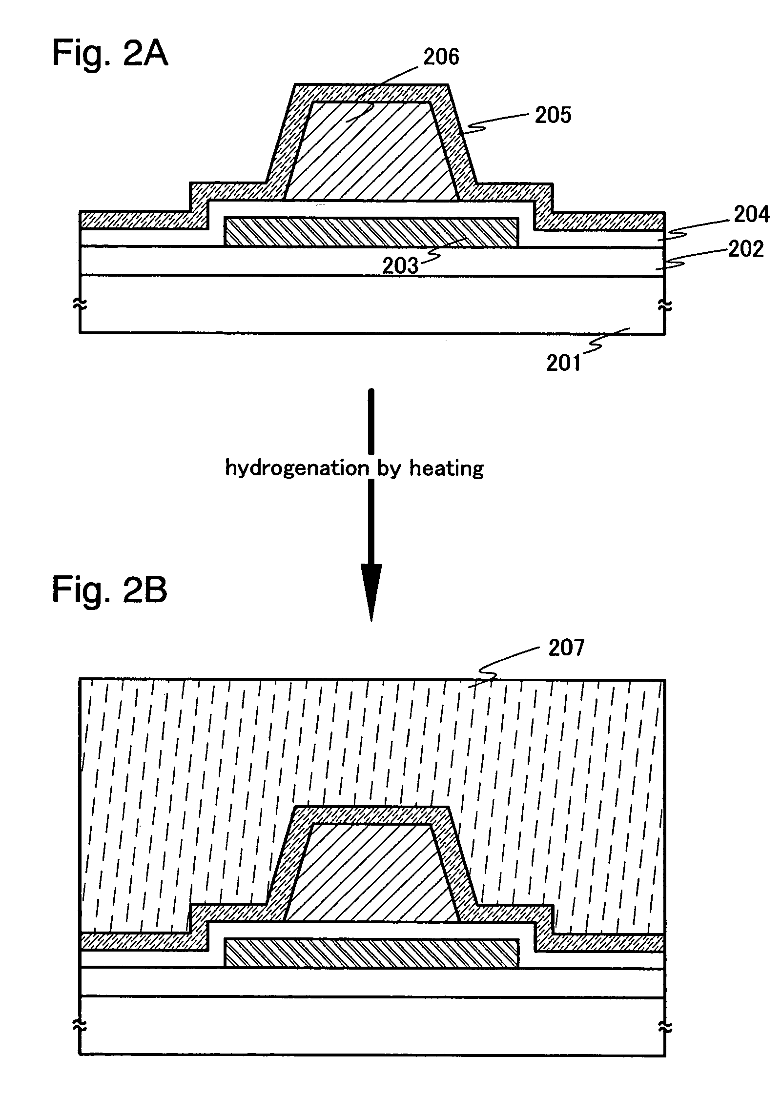
[0073]In this example, a method for manufacturing an active matrix substrate using the present invention is described with reference to FIGS. 3A to 5. An active matrix substrate comprises a plurality of TFTs, but an active matrix substrate comprising a drive circuit portion having an n-channel TFT and a p-channel TFT and a pixel portion having an n-channel TFT is described here.

[0074]A silicon nitride oxide film is formed on a substrate 300 having an insulating surface as a base film 301 by plasma CVD to have a thickness of from 10 nm to 200 nm (preferably, from 50 nm to 100 nm) and a silicon oxynitride film is laminated thereupon to have a thickness of from 50 nm to 200 nm (preferably, from 100 nm to 150 nm). In this example, the silicon nitride oxide film of 50 nm and the silicon oxynitride film of 100 nm are formed by plasma CVD. As the substrate 300, a glass substrate, a quartz substrate, a silicon substrate, a metal substrate, or a stainless substrate each of which has an insul...


PUM

PropertyMeasurementUnit
contact angleaaaaaaaaaa
temperatureaaaaaaaaaa

Abstract

An object of the present invention is to increase adhesiveness between thin films, particularly a high molecular film formed on an insulating surface, and the present invention provides a semiconductor device with high reliability and a method for manufacturing the semiconductor device with high yield. A semiconductor device of the present invention comprises a laminate structure formed in close contact with an organic insulating film on a hydrophobic surface of an inorganic insulating film including silicon and nitrogen. A film having the hydrophobic surface is an insulating film having a contact angle of water of equal to or more than 30°, preferably of equal to or more than 40°.

Description

BACKGROUND OF THE INVENTION[0001]1. Field of the Invention[0002]The present invention relates to a semiconductor device that is a device that can function by using semiconductor characteristics (for example, a display device, a semiconductor circuit, and electronics) and to a method for manufacturing the semiconductor device.[0003]2. Related Art[0004]A liquid crystal molecule, a pixel electrode, a light-emitting layer, and the like which are display-related parts are laminated over an interlayer film. Therefore, the interlayer film is required to have a smooth surface to prevent an orientation defect of liquid crystal molecules, an inhomogeneous electric field, a minute defect of a light-emitting layer due to unevenness of a pixel electrode, and the like.[0005]An organic insulating film is used as the interlayer film over an inorganic insulating film because of its good smoothness (for instance, Reference 1: Japanese Unexamined Patent Publication No. Hei10-48607). An organic insulat...

Claims


Application Information

Patent Timeline
Patent Type & Authority Patents(United States)
IPC IPC(8): H01L23/58G02F1/1333G02F1/1343H01L21/312H01L21/318H01L21/77H01L21/84H01L27/08H01L27/12H01L29/786
CPCH01L27/12H01L27/1248H01L29/78603
Inventor MURANAKA, KOJI
Owner SEMICON ENERGY LAB CO LTD
Why Eureka
Try Eureka