

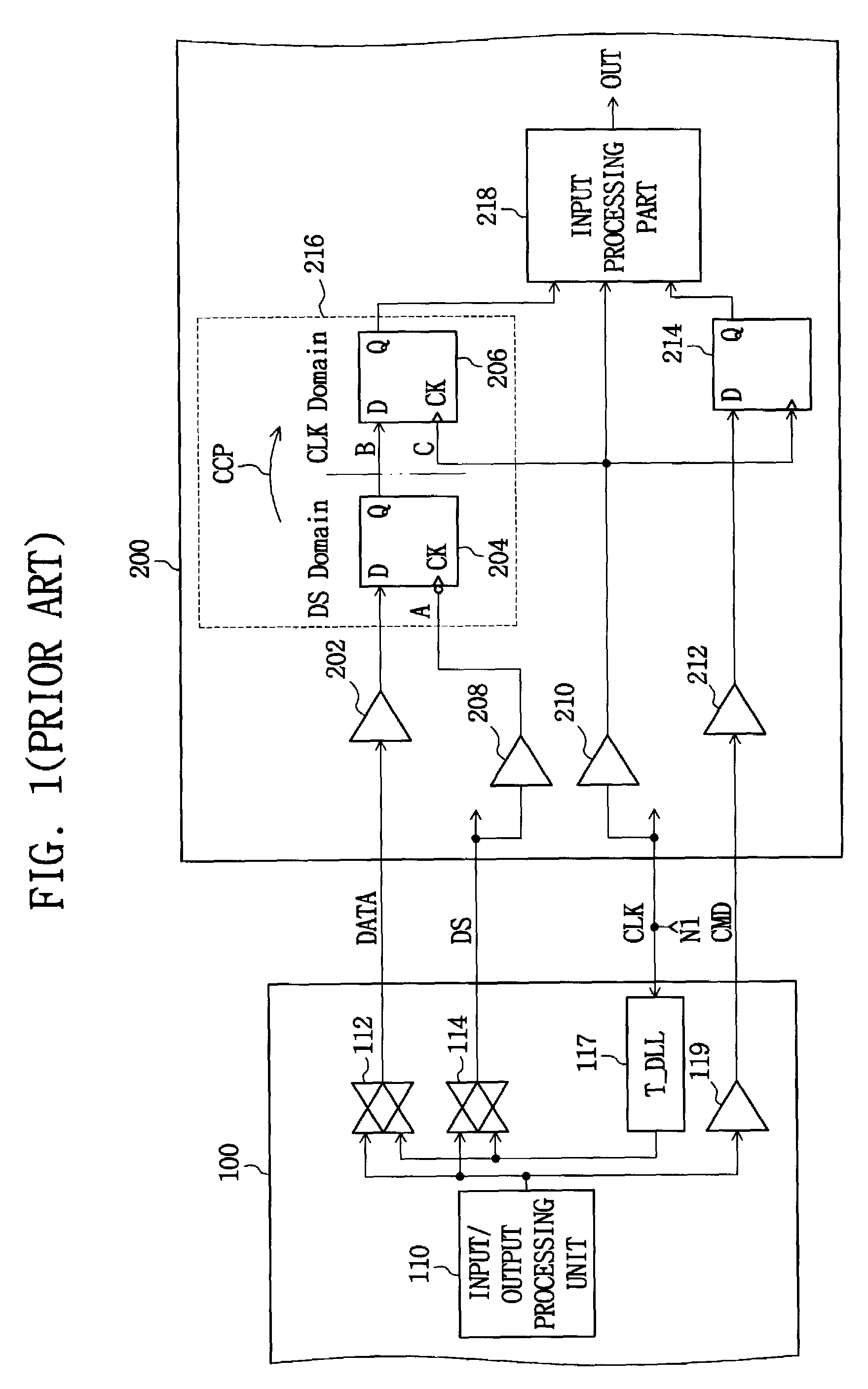
Multi-clock domain data input-processing device having clock-receiving locked loop and clock signal input method thereof
a clock signal and data input technology, applied in the field of data inputprocessing methods, can solve the problems of jitter in the dlls and complicate high frequency operations, and achieve the effect of reducing the restriction of high frequency operations and maximizing the timing margin of the clock conversion par
- Summary
- Abstract
- Description
- Claims
- Application Information
AI Technical Summary
Benefits of technology
Problems solved by technology
Method used
Image

Examples
second embodiment
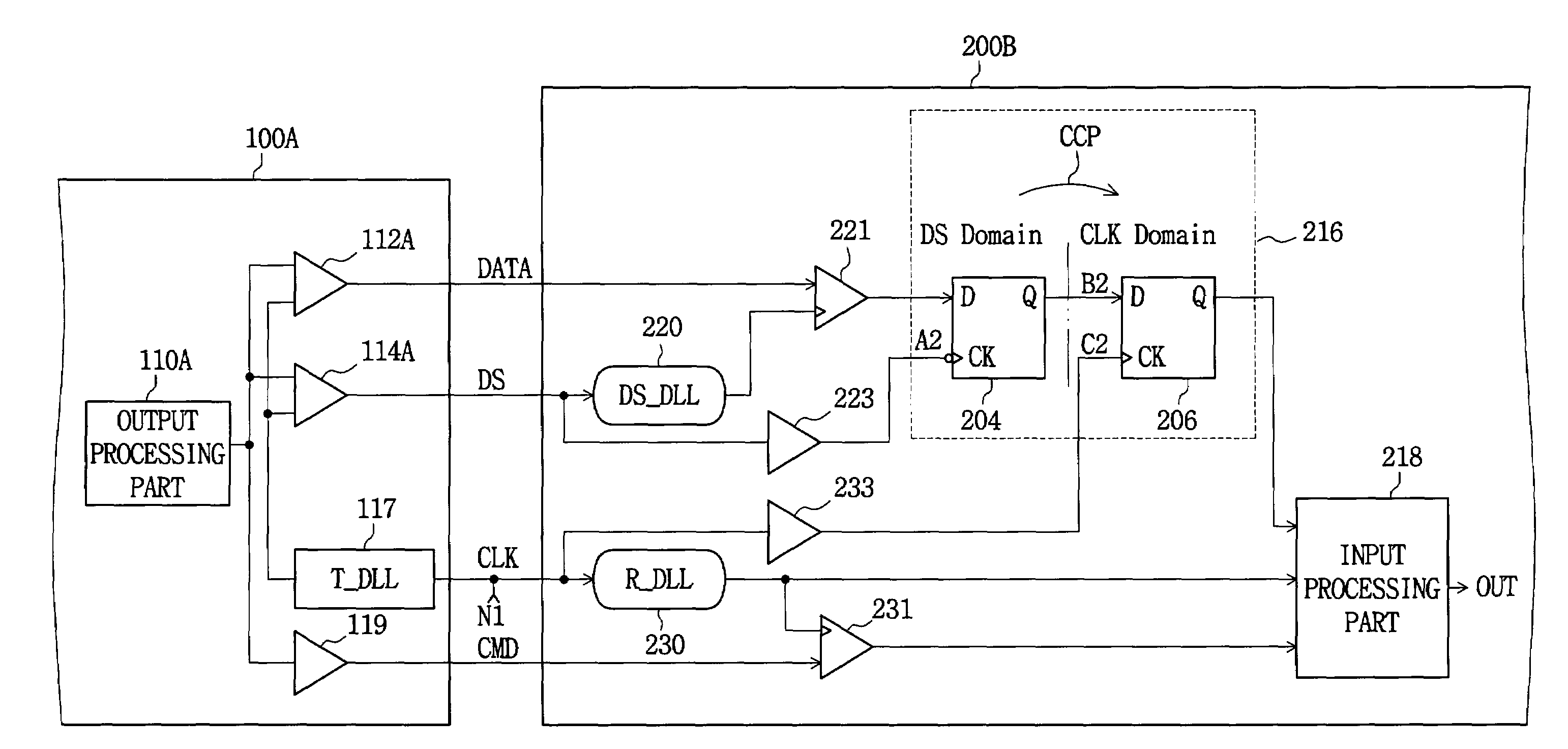
[0067]FIG. 11 illustrates a block diagram of a data input-processing unit having a signal-receiving DLL in accordance with the present invention. As shown in FIG.11, the data input-processing unit includes a clock signal-receiving synchronous circuit R_DLL 230 which generates a signal-receiving internal clock ICLK as an output clocking signal. By phase-delaying the second clock signal CLK by a predetermined time; a data input part 216 inputs data in sequential response to the first clocking signal DS that is applied simultaneously with the application of the data and to the second clocking signal CLK that is applied at a timing different from that of the first clock signal DS. An input-processing part 218 processes the data output from the data input part 216 in response to the signal-receiving internal clock ICLK of the clock signal-receiving synchronous circuit (clock signal receiving locked loop) R_DLL 230.
[0068]The structure of FIG. 11 preferably includes only a clock signal-rec...
third embodiment
[0069]FIG. 12 illustrates a block diagram of a data input-processing unit having a signal-receiving DLL according to the present invention. The structure includes only DS_DLL 220 rather than the R_DLL 230 and DS_DLL 220 combination of the preferred embodiment. As in the other embodiments, the clocking signal bypasses the DS_DLL 220, and externally received data strobe signal DS is directly applied to the signal-receiving clock conversion part CCP through a buffer 223.
[0070]FIGS. 13 and 14 illustrate representative DLLs, such as R_DLL 230 and DS_DLL 220 shown in FIGS. 9, 11 and 12. As shown in FIG. 13, a DLL (i.e., 220, 230) may include: a signal-receiving buffer 211, which receives an input clock signal IN; a variable delay unit 213, which outputs an output clock signal OUT by delaying a signal-receiving clock signal RCLK output from the signal-receiving buffer 211 in response to an applied digital control data CON; a phase detector 215, which detects a difference in the phase betwe...
PUM
 Abstract
Description
Claims
Application Information