Molded package and semiconductor device using molded package

a technology of semiconductor devices and molded packages, which is applied in the direction of semiconductor devices, semiconductor/solid-state device details, electrical apparatus, etc., can solve the problems of affecting the optical properties of light emitting devices, cracking at the interface, and resin falling out of molded packages, so as to improve the color rendering properties of mixed light

Active Publication Date: 2006-05-16
NICHIA CORP
View PDF6 Cites 79 Cited by
  • Summary
  • Abstract
  • Description
  • Claims
  • Application Information

AI Technical Summary

Benefits of technology

[0031]Another example of the fluorescent material comprises N, at least an element selected from Be, Mg, Ca, Sr, Ba, and Zn, and at least an element selected from C, Si, Ge, Sn, Ti, Zr, and Hf, and activated with at least an element selected from the rare earth elements. The fluorescent material absorbs a part of the light emitted from the light emitting el

Problems solved by technology

However, the thermal expansion coefficients of the metal member exposed in the recess of the molded package and the resin which encloses the recess are different, and so problems such as cracking at their interface occur.
Such cracking may result in the resin falling out of from the molded package.
Also, a gap created by the cracking adversely affects the optical properties of the light emit

Method used


Image

  • Molded package and semiconductor device using molded package
  • Molded package and semiconductor device using molded package
  • Molded package and semiconductor device using molded package

Examples


embodiment 1

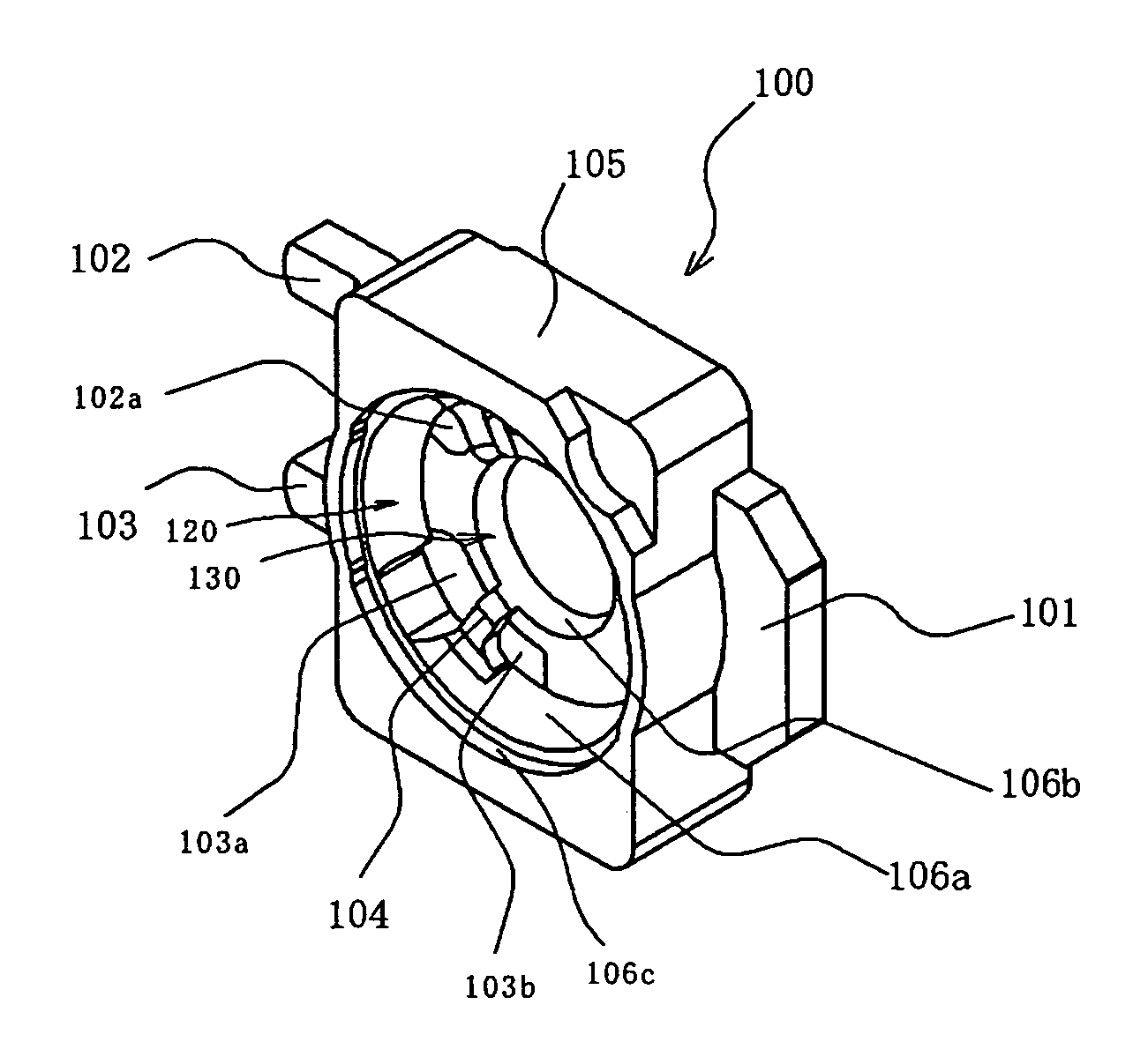
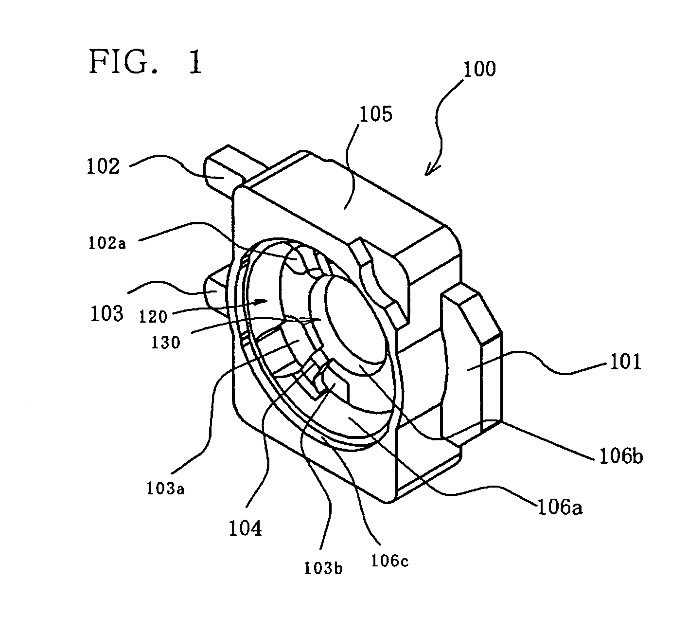
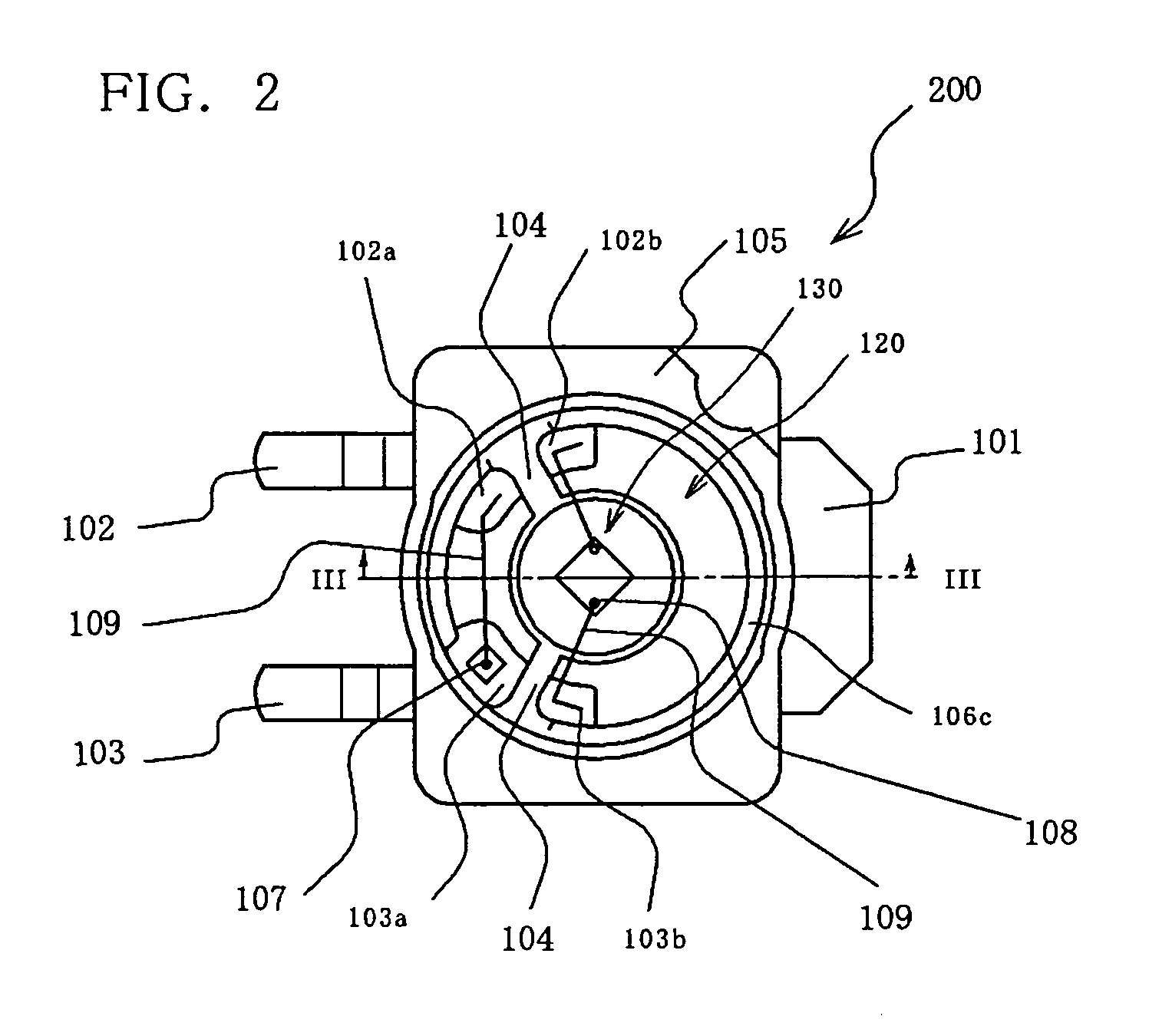
[0044]FIG. 1 shows a schematic perspective view of a molded package according to the present embodiment. FIG. 2 is a schematic top view showing the semiconductor device 200 according to the present embodiment. FIG. 3 shows a schematic cross sectional view taken along dotted line III—III of FIG. 2. FIG. 4 shows a schematic rear view of a molded package shown in FIG. 1 and FIG. 2.

[0045]That is, the molded package 100 of the present invention includes a first metal member 101 and a second metal member 102, and a third metal member 103. The metal members are oppositely disposed, and insulated from each other by the mold member 105. Here, the molded package is formed by way of integral molding so that one end of the first metal base 101, one end of the second metal base 102, and one end of the third metal base 103 are inserted in the mold member 105 and respective other ends are protruded from the outer surface of the mold member 105.

[0046]Also, a recess (first recess 120) is formed by t...

embodiment 2

[0057]FIG. 5 shows a schematic top view of a semiconductor device 300 of the present embodiment, and FIG. 6 shows a schematic cross sectional view taken along dotted line VI—VI of FIG. 5. FIG. 7 shows a schematic top view of a semiconductor device of another embodiment, and the FIG. 8 shows a schematic cross sectional view taken along dotted line VIII—VIII of FIG. 7. FIG. 9 shows a rear view of the semiconductor device shown in FIG. 7. FIG. 10 shows a schematic top view of a semiconductor device of yet another embodiment, and FIG. 11 shows a schematic cross sectional view taken along dotted line XI—XI of FIG. 10.

[0058]A molded package according to the present embodiment includes a first metal member 101, second metal member 102, a third metal member 103 and an encapsulating member 302. The metal members are oppositely disposed, and insulated from each other by the mold member 105, as described in the embodiment above. Here, the first metal member 101, the second metal member 102, an...

example 1

[0215]As shown in FIG. 2, a surface mounting type of light emitting device (SMD) is formed. The LED chip 108 is a nitride semiconductor light emitting element including an active layer of an In0.2Ga0.8N semiconductor with a monochromatic emission peak being a visible color of 475 nm.

[0216]In more detail, the LED chip 108 is formed by growing the nitride semiconductors on a clean sapphire substrate by MOCVD method using TMG (trimethyl-gallium) gas, TMI (trimethyl-indium) gas, nitrogen gas and dopant gas along with a carrier gas. The layers of the n-type nitride semiconductor or the p-type nitride semiconductor are formed by switching the dopant gas between SiH4 and Cp2Mg.

[0217]The elemental structure of the LED chip 108 of the present example is sequentially formed on a sapphire substrate. The layers include a GaN layer of an undoped nitride semiconductor, a contact layer of n-type GaN layer having an n-type electrode doped with Si, a GaN layer of undoped nitride semiconductor, and a...


PUM


Abstract

A molded package comprises at least a first metal member, a second metal member, and a third metal member. Each member includes an end portion inserted into a mold member where a recess is formed and another end portion protruding from an outer wall of the mold member. A portion of each main surface of the metal members is exposed from the mold member in the bottom of the recess. A portion of each main surface can be also divided into at least two bonding regions by a wall portion comprising part of the mold member. A semiconductor device of the present invention comprises the molded package, a semiconductor component, and an encapsulating member covering the semiconductor component, and has a high reliability.

Description

BACKGROUND OF THE INVENTION[0001]1. Field of the Invention[0002]The present invention relates to a molded package comprising a metal member such as a lead electrode which supplies electric power to a semiconductor element incorporated into the mold member by way of insert molding, and further to a semiconductor device using the molded package as a support member.[0003]2. Discussion of the Related Art[0004]Conventionally, there has been a semiconductor device in which a light emitting semiconductor element, a protective element which protects the light emitting semiconductor element from a damage caused by overvoltage, and a plurality of semiconductor elements are housed in a recess of a molded package. In such a semiconductor device, a semiconductor element and a conductive wire which supplies electric power to the semiconductor element are connected to the surface of a metal member such as a lead electrode exposed in the recess of the molded package by way of die bonding or wire bo...

Claims


Application Information

Patent Timeline
IPC IPC(8): H01L23/28H01L23/495H01L23/498H01L25/16H01L33/32H01L33/50H01L33/56H01L33/62
CPCH01L23/49562H01L23/49861H01L25/167H01L33/62H01L2924/07802H01L2924/3025H01L2224/48465H01L2924/12041H01L2924/01322H01L2924/01068H01L2924/01067H01L2924/01066H01L2924/01021H01L2924/01019H01L24/48H01L2224/48091H01L2224/48247H01L2924/01004H01L2924/01012H01L2924/0102H01L2924/01025H01L2924/01057H01L2924/01063H01L2924/01078H01L2924/01079H01L2924/19041H01L2924/00014H01L2924/00H01L2924/12035H01L2924/12042H01L2924/12036H01L2224/45015H01L2224/45124H01L2224/45144H01L2224/45147H01L2224/45169H01L2224/48097H01L2924/181H01L2224/49171H01L24/49H01L2924/20752H01L2924/20753H01L2224/45099H01L2924/207H01L2224/48095
Inventor NAKASHIMA, SHINTARO
Owner NICHIA CORP
Why Eureka
Try Eureka