
Device for supplying control signals to memory units, and a memory unit adapted thereto

Inactive Publication Date: 2006-05-16
POLARIS INNOVATIONS
View PDF5 Cites 0 Cited by
  • Summary
  • Abstract
  • Description
  • Claims
  • Application Information

AI Technical Summary

Benefits of technology

[0007]It is the object of the present invention to provide a device for supplying control signals to memory units of a memory module, and a memory unit adapted thereto, said device and said memory unit permitting rapid, reliable accessing of the memory units with high transmission rates.
[0021]The new architecture of the control-signal busses, especially of the command / address bus of DRAM memory modules, according to the present invention permits a reduction of signal displacement and an increase in the transmission rate on the command / address bus in the memory module. The present invention makes it possible to drive the command / address bus at double data rate, i.e. the same data rate at which the data bus is driven. In addition, the architecture according to the present invention permits a reduction of the number of connections of the memory module, since not each individual memory chip receives all the positions of the command / address signals. In view of the improved topology, the present invention permits the reduction of layers in the printed module board. Furthermore, a separate register or buffer IC (IC=integrated circuit) can be dispensed with, when register or buffer drivers are provided on the respective circuit chips so as to realize the redrive of parts of the C / A signals between the circuit chips.

Problems solved by technology

The problems referred to especially arise, to a greater degree, in the case of memory modules with high access rates and access frequencies, e.g. DDR memory modules (DDR=Double Data Rate), which are normally constructed as DIMM architecture (DIMM=Dual In-line Memory Module).

Method used


Image

  • Device for supplying control signals to memory units, and a memory unit adapted thereto
  • Device for supplying control signals to memory units, and a memory unit adapted thereto
  • Device for supplying control signals to memory units, and a memory unit adapted thereto

Examples


Embodiment Construction

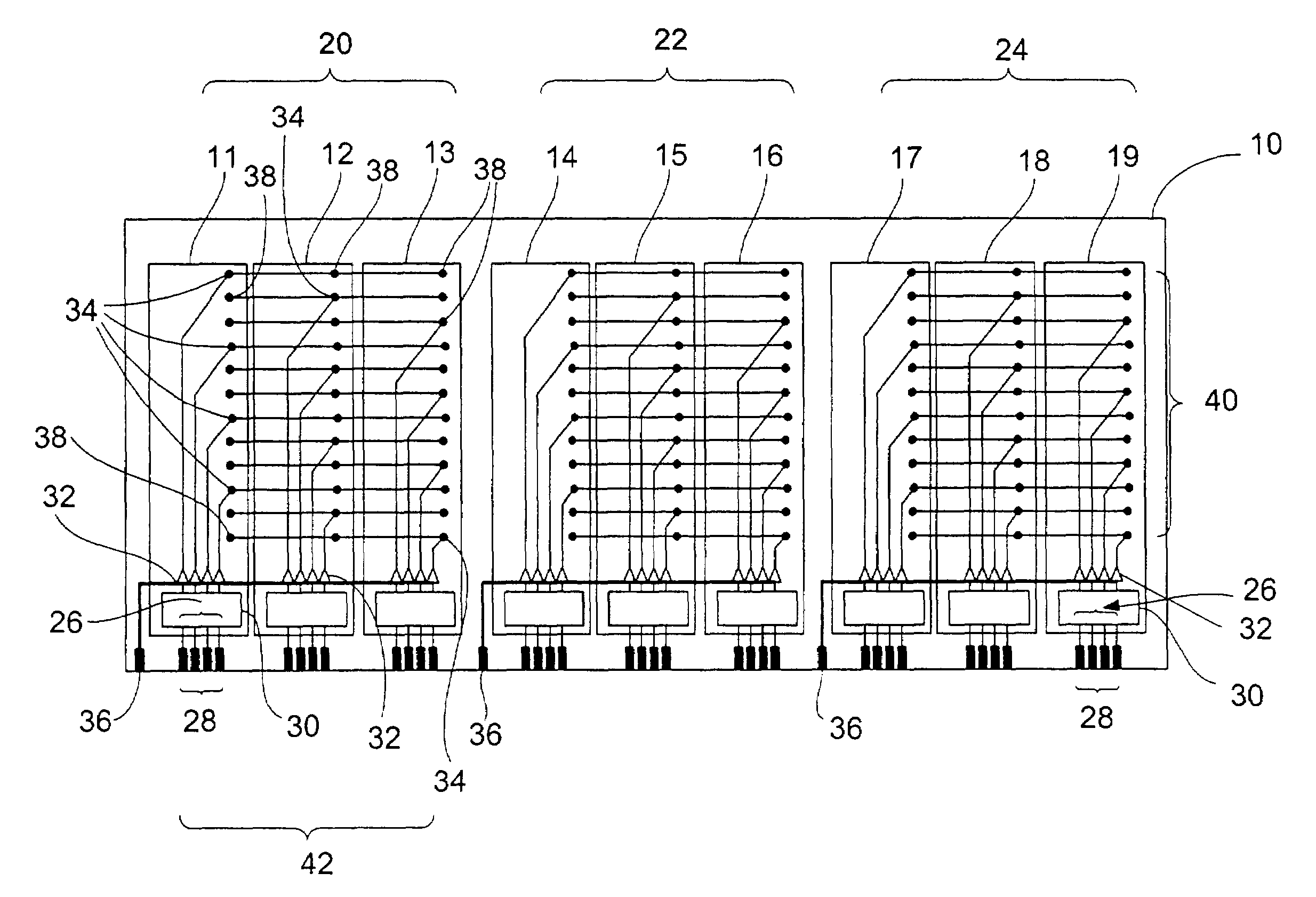
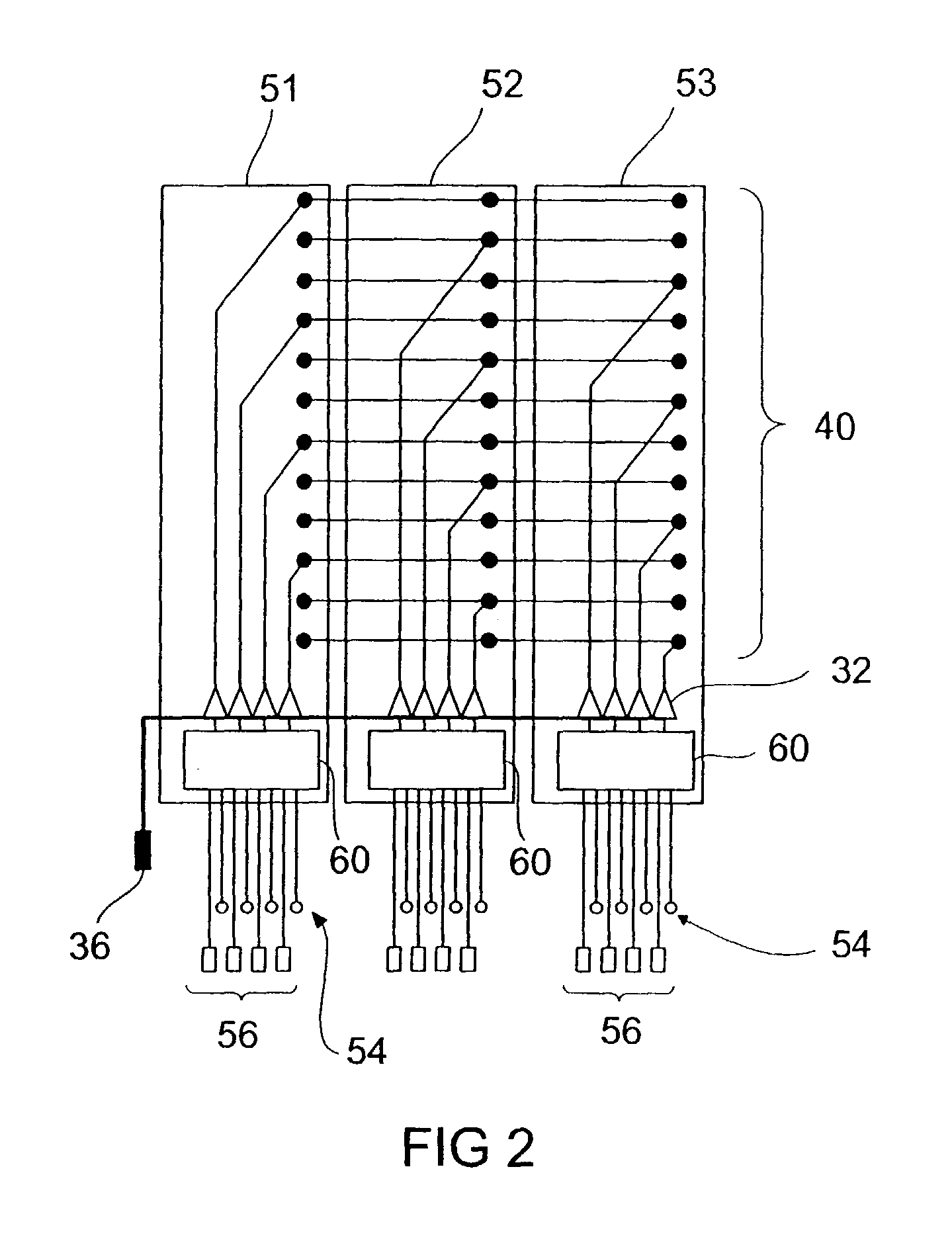
[0026]Making reference to the figures enclosed, the present invention will be explained in detail in the following on the basis of command / address bus and data bus architectures for a DRAM memory module in the case of which C / A signals having a width of 24 bits and data signals having a width of 8 bits are used. It is, however, clear that the present invention can also be used for other memory architectures with control signals and data signals having other bit widths.

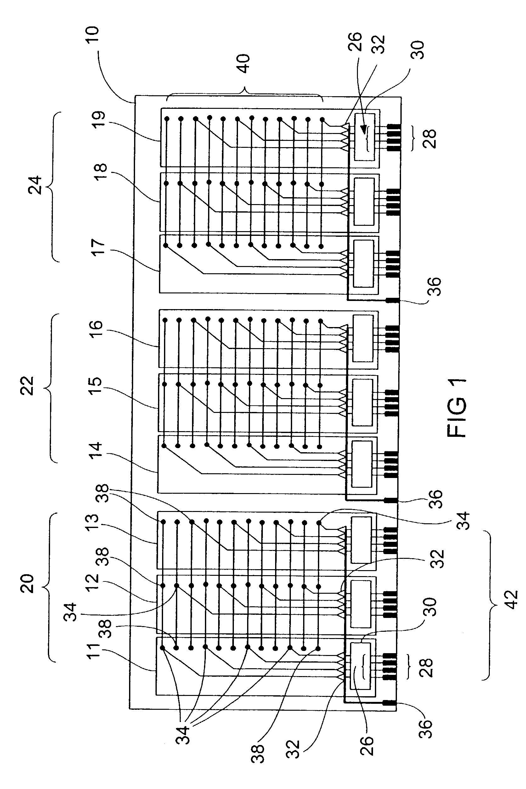
[0027]As can be seen in FIG. 1, a memory module 10 comprises nine memory chips 11 to 19. The memory chips 11 to 13 form a first group 20, the memory chips 14 to 16 form a second group 22 and the memory chips 17 to 19 form a third group 24. Each memory cell 11 to 19 has eight first inputs, the first inputs of the memory chips 11 and 19 being exemplarily designated by reference numeral 26. It should here be pointed out that, for the sake of clarity, only four of the respective inputs 26 cell are shown in the figures. Sim...


PUM


Abstract

A device for supplying control signals to memory units of a memory module comprises a first bus section for supplying a first part of the control signals to a first memory unit. In addition, a second bus section is provided for supplying a second part of the control signals to a second memory unit. Finally, the device comprises redrive means for redriving the first part of the control signals from the first memory unit to the second memory unit and for redriving the second part of the control signals from the second memory unit to the first memory unit. A memory unit for such a device for supplying control signals comprises first inputs for receiving a first part of the control signals from a memory control, second inputs for receiving a second part of the control signals from at least one other memory unit, and outputs for redriving said first part of the control signals to said at least one other memory unit.

Description

BACKGROUND OF THE INVENTION[0001]1. Field of the Invention[0002]The present invention relates to a device for supplying control signals to memory units of a memory module, and, in particular, to a device which is suitable for supplying command / address signals to memory chips arranged on a memory module. In addition, the present invention relates to a memory unit adapted to such a device, in particular a memory unit which is used as memory chip of a memory module.[0003]2. Description of the Related Art[0004]Conventional memory modules consist of a plurality of memory chips which are arranged on a common board and which form a memory module. For accessing the individual memory chips, command / address buses and data buses are provided in addition to suitable clock lines. Conventional DRAM memory modules (DRAM=Dynamic Random Access Memory), for example, have such a configuration. Both data signals and control signals are supplied to the memory module making use of an external memory cont...

Claims


Application Information

Patent Timeline
IPC IPC(8): G06F13/00G06F13/14G06F13/36G11C5/00G11C7/22G11C8/06
CPCG11C5/04
Inventor KUZMENKA, MAKSIM
Owner POLARIS INNOVATIONS
Learn More