Semi-custom-made semiconductor integrated circuit device, method for customization and method for redesign

a semi-custom-made, semiconductor technology, applied in logic circuits using specific components, pulse techniques, instruments, etc., can solve the problems of uneconomical resource utilization, uneconomical resource utilization, and large area consumed by via-holes b>4/b>v, and achieve reduced contact resistance and parasitic capacitance of signal paths, and high degree of freedom

Inactive Publication Date: 2006-05-16
RENESAS ELECTRONICS CORP
View PDF20 Cites 27 Cited by
  • Summary
  • Abstract
  • Description
  • Claims
  • Application Information

AI Technical Summary

Benefits of technology

[0021]It is therefore an important object of the present invention to provide a semi-custom-made integrated circuit device, which offers a high degree of freedom and signal paths reduced in contact resistance and parasitic capacitance to designers who customize it.

Problems solved by technology

Thus, the first problem inherent in the first prior art metal option is uneconomical usage of the resources.
However, the via-holes 4V still consumes a wide area.
Thus, the first problem inherent in the second prior art metal option is also the uneconomical usage of the resources.
The first and second prior arts metal options are not desirable from the viewpoint of the signal propagation characteristics.
Thus, the second problem inherent in the first prior art metal option is the poor signal propagation characteristics.
Thus, the second problem inherent in the second prior art metal option is also poor signal propagation characteristics.
If the signal propagation paths are assigned to clock signals to certain clocked circuits, the skew is serious due to the large difference between the signal paths.
Thus, the third problem inherent in the first and second prior art metal options is the unequal signal propagation paths.

Method used


Image

  • Semi-custom-made semiconductor integrated circuit device, method for customization and method for redesign
  • Semi-custom-made semiconductor integrated circuit device, method for customization and method for redesign
  • Semi-custom-made semiconductor integrated circuit device, method for customization and method for redesign

Examples


Embodiment Construction

Structure of Semi-Custom-Made Integrated Circuit Device

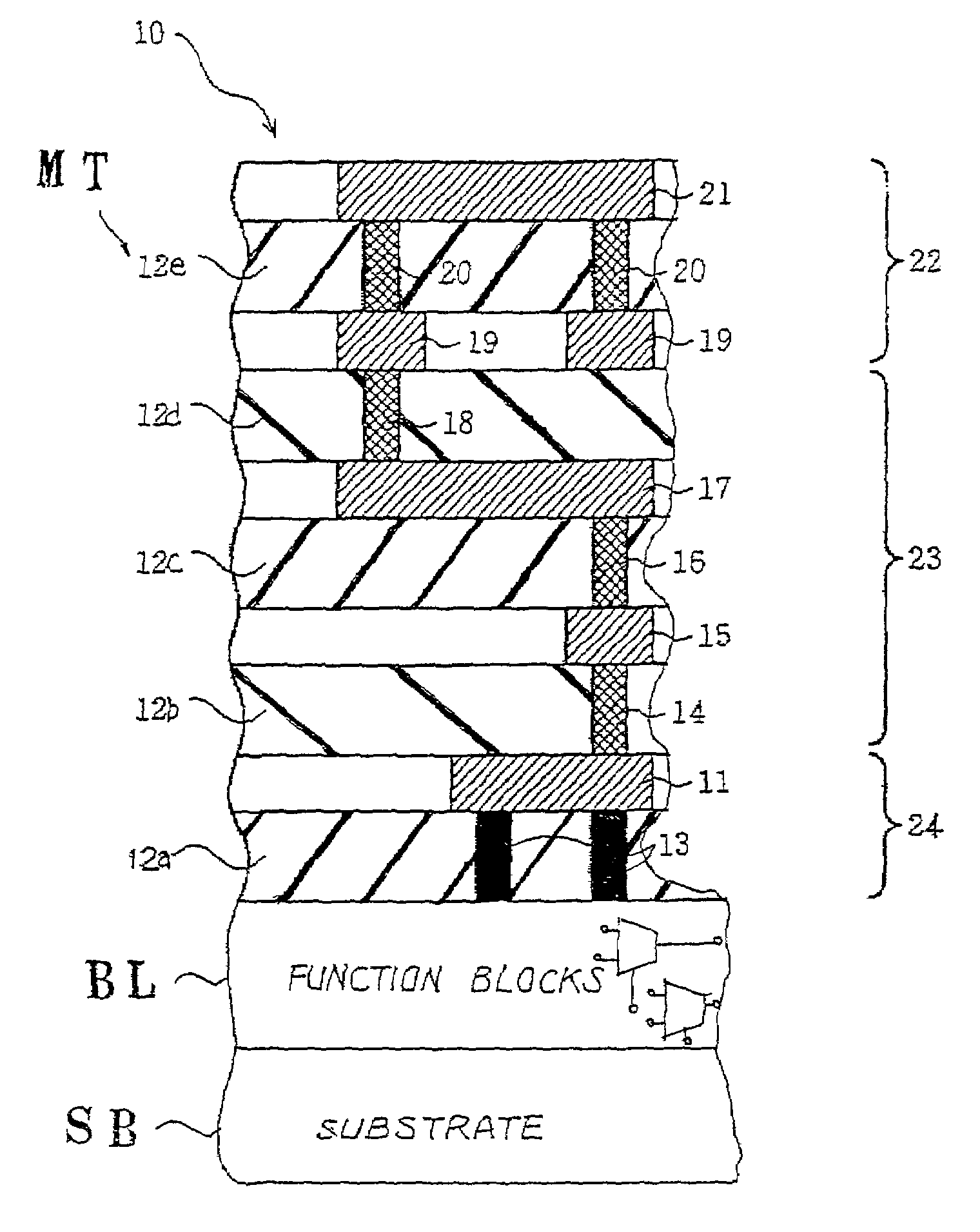
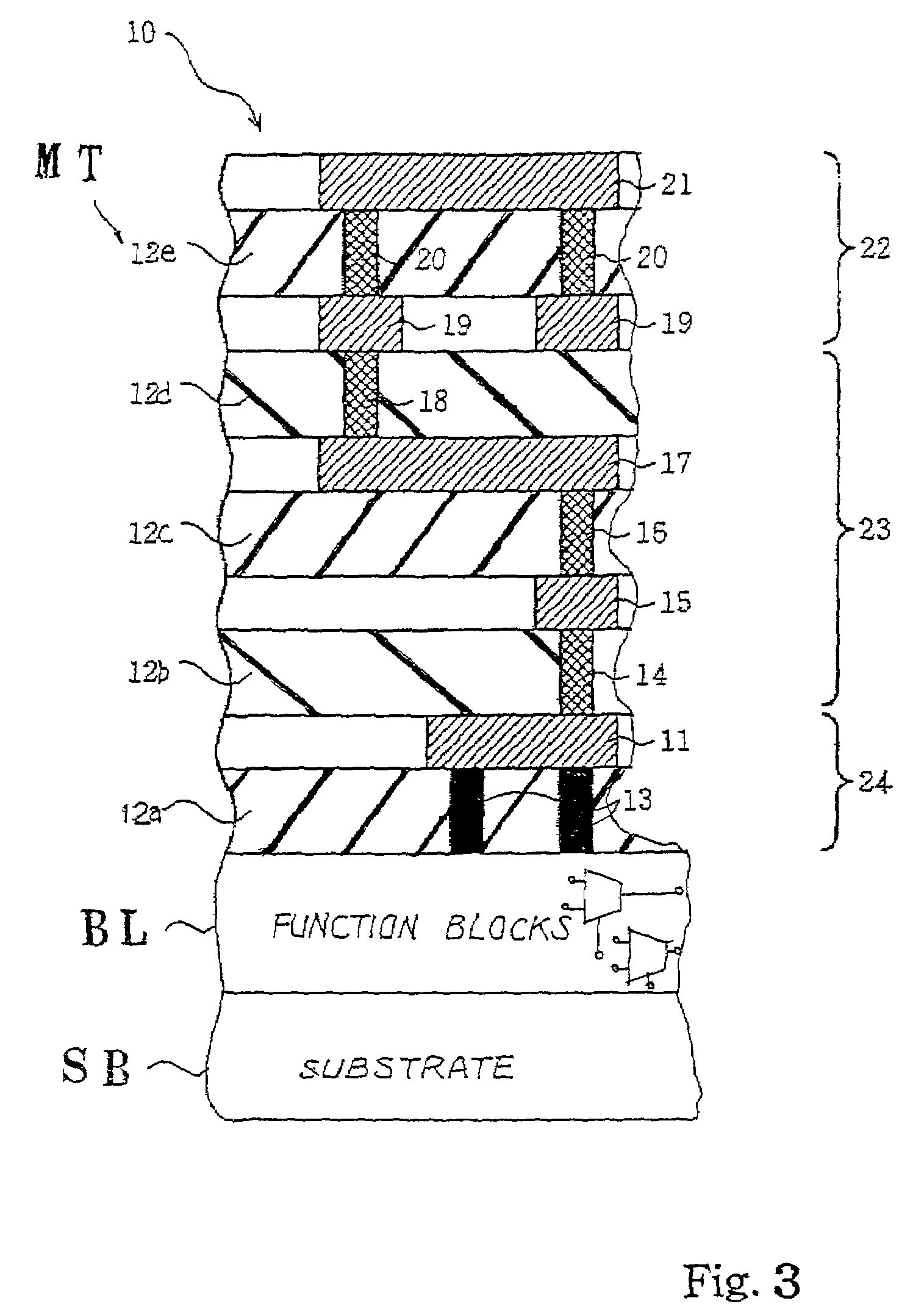
[0045]Referring to FIG. 3 of the drawings, an ASIC embodying the present invention is designated by reference numeral 10. The ASIC 10 is fabricated on a semiconductor substrate SB. The ASIC 10 is broken down into a function block layer BL and a multi-layered structure of metallization MT. The function block layer BL includes plural function blocks, and universal logic cells form in combination each of the function blocks. Although a large number of universal logic cells are incorporated in the function blocks, only two universal logic cells are shown in FIG. 3. Each function block may have one of the circuit configurations described in connection with the background of the invention.

[0046]The multi-layered structure of metallization MT includes five metallization layers 11, 15, 17, 19 and 21 and inter-layered insulating layers 12a, 12b, 12c, 12d and 12e. In detail, the function block layer BL is covered with the first inter-laye...


PUM


Abstract

An ASIC includes a function layer formed with plural universal logic cells, a common layer formed with conductive strips connected to the universal logic cells and common to other ASICs and a customized layer having at least two metallization layers assigned to conductive strips extending in certain directions parallel to one another and other conductive strips extending in perpendicular directions to the certain directions, respectively, and an inter-layered insulating layer formed with conductive plugs selectively connected between the conductive strips and the other conductive strips, wherein the conductive strips have respective values of length such that the conductive plugs are located on both ends thereof, whereby the conductive strips, other conductive strips and the conductive plugs form plural signal paths reduced in total contact resistance and parasitic capacitance.

Description

FIELD OF THE INVENTION[0001]This invention relates to a semiconductor integrated circuit device and, more particularly, to a semi-custom-made semiconductor integrated circuit device, a method for customization and a method for redesign the semi-custom-made semiconductor integrated circuit device.DESCRIPTION OF THE RELATED ART[0002]ASIC (Application Specific Integrated Circuit) is defined as “integrated circuits customized for specific users. The ASICs are broken down into two categories. The first category is referred to as “cell-based integrated circuit”, and the other category is referred to as “gate array”. The cell-based integrated circuit requires a set of customized photo-masks for a complete process, i.e., from the fabrication of circuit components to the metallization. On the other hand, the gate arrays are fabricated on master slices common to different users. Circuit components such as logic gates are fabricated on the master slice, and are programmable through the metalli...

Claims


Application Information

Patent Timeline
Patent Type & Authority Patents(United States)
IPC IPC(8): G06F17/50H01L21/822H01L21/82H01L27/04H01L27/118
CPCH01L27/118
Inventor MIZUNO, MASAHARUMAEDA, NAOTAKA
Owner RENESAS ELECTRONICS CORP
Why Eureka
Try Eureka