
Method for producing a tag or a chip card having a coil antenna

Inactive Publication Date: 2006-05-23
ASSA ABLOY AB
View PDF15 Cites 18 Cited by
  • Summary
  • Abstract
  • Description
  • Claims
  • Application Information

AI Technical Summary

Benefits of technology

[0009]It is thus the aim of this present invention to propose a method with a device for producing a tag that encompasses an antenna or a coil or some other arrangement that not only drastically simplifies but substantially minimises the costs involved in producing and arranging the coil on the tag or chip card in this way.
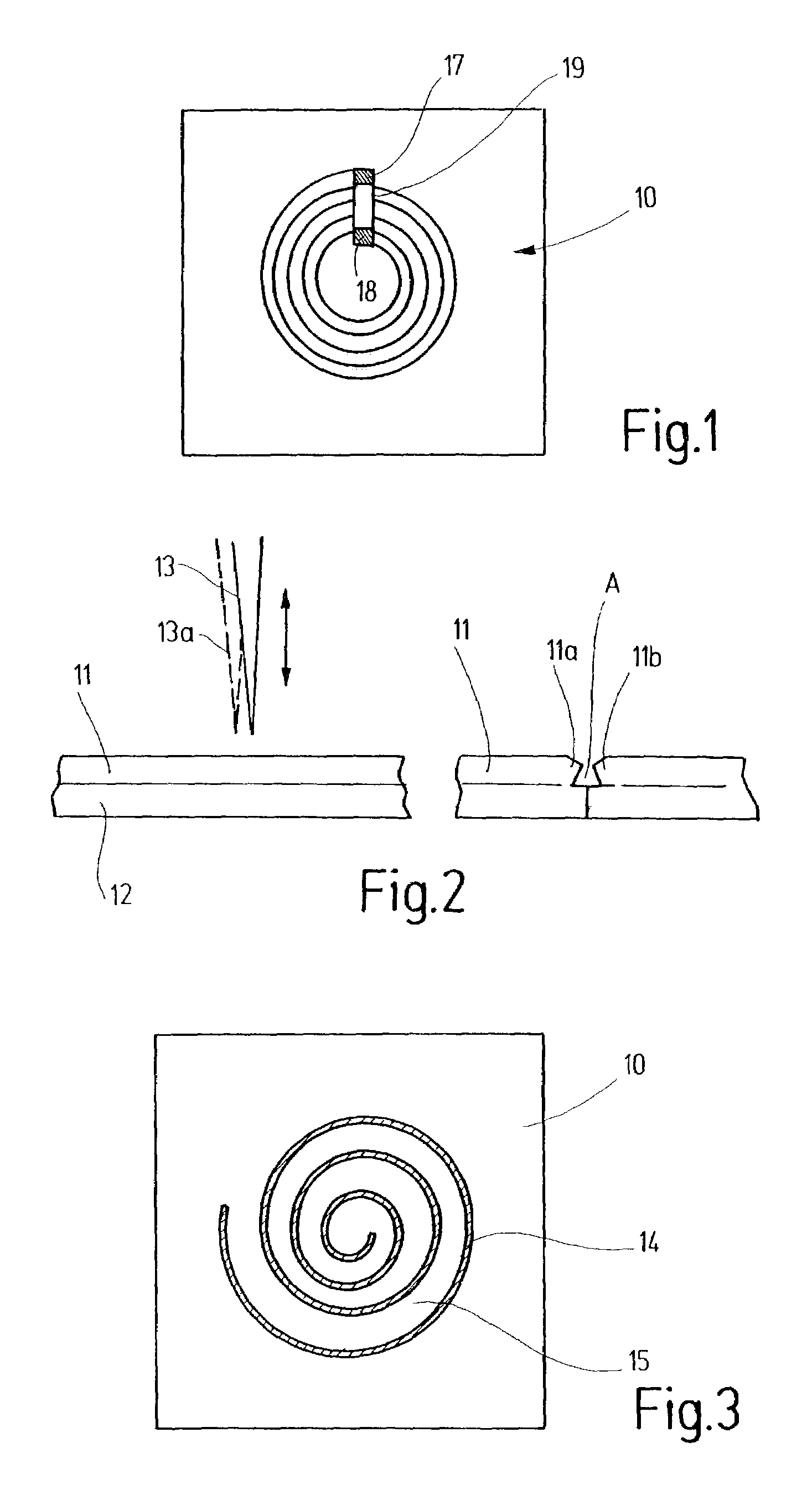
[0011]This die-cutting process allows the antenna to be produced in any shape, also ones which match the shape of the tag; this means that in the preferred and therefore also the simplest embodiment, no post-processing steps are required.
[0013]If the preferred embodiment of the present invention is employed, no die-cut parts have to be removed during the die-cutting process in order to produce the antenna, a process which would necessitate employing an additional operation involving a gripping action—a single die-cutting process is sufficient, for instance in a spiral shape, in order to immediately produce a spiral wound antenna on the copper-coated substrate, the two ends of which only need to be attached to the respective chip module, for instance by crimping or soldering if desired.
[0016]Not only does the invention make it possible to manufacture such tags, which are now required in great numbers, considerably faster in comparison with, for instance, the step-by-step wire application method involving intermediate attachments in accordance with both the publications cited at the outset, but also substantially reduces the number of processing stages required in comparison with the known etching method. In this way and in conjunction with the structural simplification, it represents an effective reduction in costs.

Problems solved by technology

However, when attaching or applying such coils or antennas to each substrate, there are certain problems that significantly increase the cost of such tags that are now required in their millions.
In particular, these involve the application of photoresist to vapour-deposited or otherwise applied conductive layers, then their exposure using masks and the removal of intermediate layers by means of etching, all of which make the production of such tags considerably more expensive, especially when one considers the large number of units common in this field.
Both methods of attaching the wire are complicated as well as time-consuming, with WO 95 / 26538 also proposing that the coil wire be connected to the first terminal pad of a chip located on the chip card at the same time as it is being laid.

Method used


Image

  • Method for producing a tag or a chip card having a coil antenna
  • Method for producing a tag or a chip card having a coil antenna
  • Method for producing a tag or a chip card having a coil antenna

Examples


Embodiment Construction

[0023]The basic idea behind the present invention is to create an extended sequence of antenna or coil windings or turns by die-cutting these from a flat layer of electrically conductive material, whereby said windings or turns can be employed in the manufacture of tags or generally in the manufacture of transponder-type assemblies.

[0024]The preferred embodiment of the invention shall be described directly below in greater detail, whereby the basic material for the manufacture of the antenna is a flat foil of electrically conductive material, commonly copper or aluminium foil, which is applied or laminated onto a supporting substrate, preferably a synthetic film such as polyester.

[0025]The thickness of such a polyester film can for instance range between 50 and 250 μ, but can be set at any thickness as required, in the same manner as the thickness of the copper foil used for the actual manufacturing process is of subordinate significance and can be derived from the other parameters ...


PUM

PropertyMeasurementUnit
Electrical conductivityaaaaaaaaaa
Shapeaaaaaaaaaa

Abstract

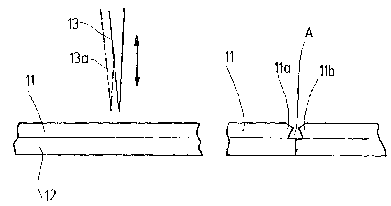
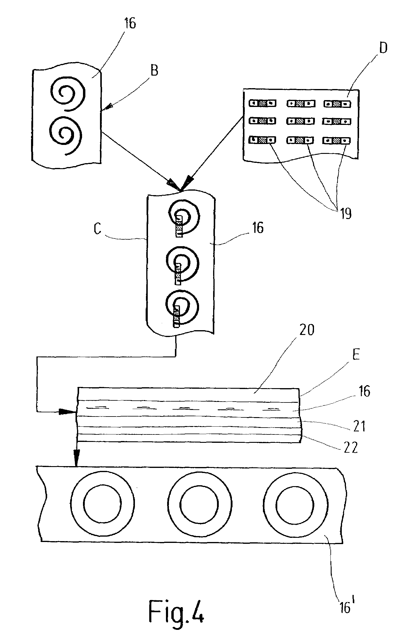
A method for manufacturing a tag encompassing an antenna or coil that is capable of at least one of wirelessly transmitting information to remote receivers and receiving information from remote transmitters. The method includes die-cutting a coil or antenna shape from an electrically conductive flat double foil having an upper electrically conductive flat foil layer of a soft, inelastic metal and a lower synthetic film substrate layer, the die-cutting including cutting with a die-cutting tool having a single die-cutting blade which matches the desired antenna or coil shape, the blade completely perforating the upper electrically conductive flat foil and at least partially separating the lower synthetic film substrate so that a gap the distance created in the flat foil by die-cutting remains after the die-cutting tool is removed. Subsequently the cut shape is bonded with additional layers including an electronic chip module.

Description

PRIORITY CLAIM[0001]This is a U.S. national stage of application No. PCT / IB01 / 00532, filed on Mar. 31, 2001. Priority is claimed on that application and on the following application: Country: Germany, Application No.: 100 16 037.9, Filed: Mar. 31, 2000.BACKGROUND OF THE INVENTION[0002]The present invention concerns a method for manufacturing a tag which encompasses an antenna or a coil. The invention further relates to an apparatus for executing the method i, and a tag encompassing an antenna or coil or a corresponding chip card.[0003]Chip cards or identification cards encompassing an antenna or a coil or similar small-scale assemblies such as for instance tags, transponder units and the like, are known in a multiplicity of embodiments. They generally serve to receive wireless information and, in some cases, to process it, but also to transmit information, for instance concerning the location, the properties of the objects connected to it and similar information (back) to the approp...

Claims


Application Information

Patent Timeline
IPC IPC(8): H01P11/00G06K19/077H01F41/04H01Q1/36H01Q1/40H05K1/16H05K3/04
CPCG06K19/07718G06K19/07749G06K19/0775H01F41/041H05K3/041Y10T29/49004Y10T29/49018Y10T29/49016H05K1/165G06K19/077
Inventor VOGT, WERNER
Owner ASSA ABLOY AB
Learn More