
Maskless middle-of-line liner deposition

a middle-of-line liner and maskless technology, applied in the field of semiconductor structure manufacturing, can solve the problems of large sub-vt (voltage threshold) leakage, low retention time, and increase the risk of shorting between the bit-line and the word-line, and achieve enhanced chemical vapor deposition

Inactive Publication Date: 2006-05-23
POLARIS INNOVATIONS LTD
View PDF13 Cites 5 Cited by
  • Summary
  • Abstract
  • Description
  • Claims
  • Application Information

AI Technical Summary

Benefits of technology

This approach reduces sub-VT leakage and the risk of shorts between bit-line and word-line, while providing cost savings by eliminating the need for a block mask, and effectively manages the MOL liner thickness to protect the crystalline silicon region.

Problems solved by technology

However, shrinking the gate length leads to a larger sub-VT (voltage threshold) leakage.
Sub-VT leakage is current leakage caused when electrical current flows underneath the gate from source to drain without opening the gate.
Sub-VT leakage allows the capacitors to leak charge causing low retention time.
Unfortunately, the contact etch often etches a portion of the gate cap silicon nitride layer in addition to etching through the MOL liner, the silicon oxide layer and the silicon nitride layer.
Etching a portion of the gate cap layer increases the risk of shorting between the bit-line and the word-line.

Method used


Image

  • Maskless middle-of-line liner deposition
  • Maskless middle-of-line liner deposition
  • Maskless middle-of-line liner deposition

Examples


Embodiment Construction

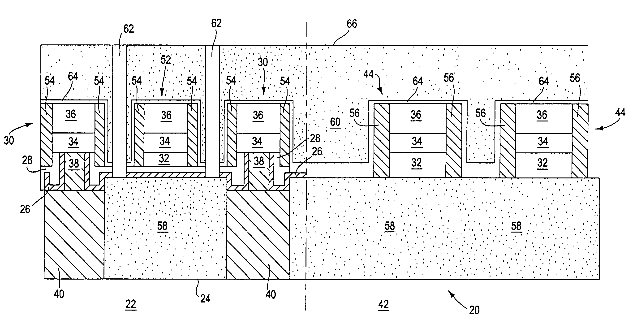
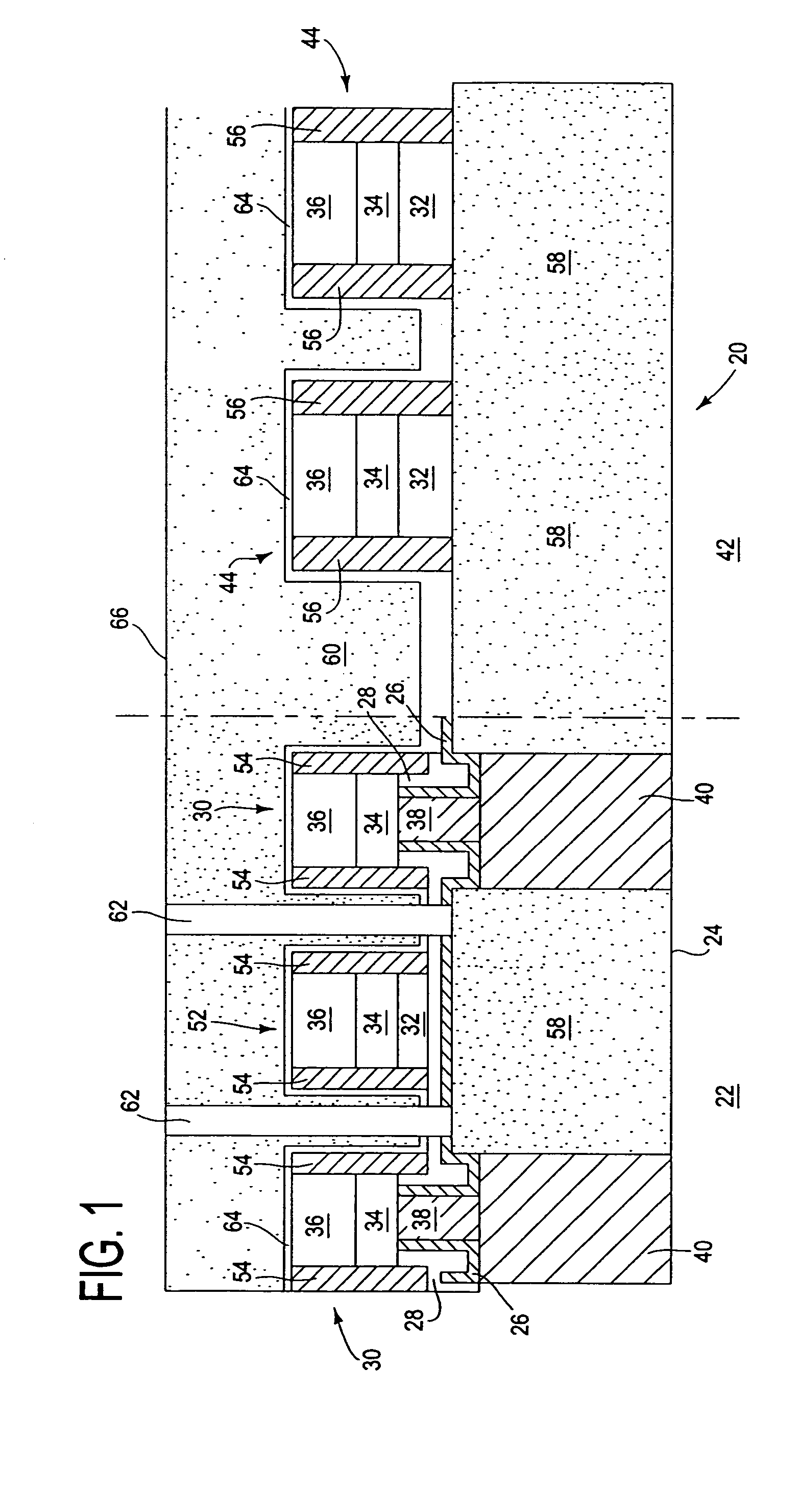
[0012]FIG. 1 shows a semiconductor structure 20 in cross-section which includes a core region 22 and a periphery region 42. The core region 22 includes a passing wordline 52 in between a plurality of vertical transistors 30 and overlying a semiconductor substrate 24. The periphery region 42 includes at least one lateral transistor 44 overlying the semiconductor substrate 24. A middle-of-line (MOL) liner 64 overlies the passing wordline 52, the vertical transistors 30, and the lateral transistor 44. In order to fill-in the gaps between features such as transistors 30, 44 and passing wordline 52, an insulative layer 60 is placed in between and above the transistors 30, 44 and passing wordline 52 as illustrated in FIG. 1. Additionally, a contact 62 passes through the insulative layer 60 to the semiconductor substrate 24.

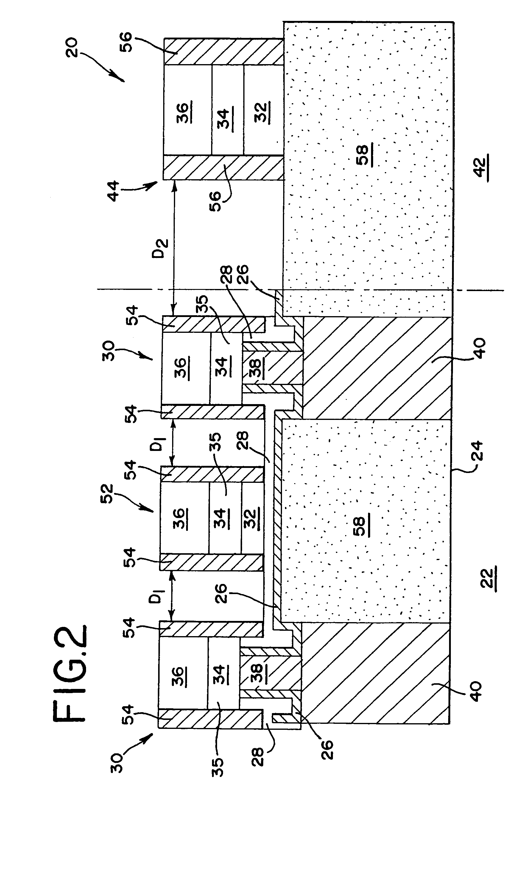
[0013]Referring to FIG. 2, the semiconductor structure 20 of the present invention is fabricated using a semiconductor substrate 24. The semiconductor substrate 24 comp...


PUM


Abstract

A process for fabricating a semiconductor structure, wherein the semiconductor structure includes a core region and a periphery region. The core region includes a plurality of transistors and the periphery region includes a plurality of transistors. The process includes depositing a middle-of-line liner using plasma enhanced chemical vapor deposition overlying the semiconductor structure. By using a plasma enhanced chemical vapor deposition the amount of MOL liner deposited in the core region and the periphery region can be controlled depending on the distances between transistors in the core region and periphery region.

Description

[0001]The present application is a divisional of U.S. application Ser. No. 10 / 210,132, filed Jul. 31, 2002 now U.S. Pat No. 6,822,301, which is hereby incorporated herein in its entirety by this reference.BACKGROUND[0002]This invention relates generally to semiconductor devices. In particular, the present invention relates to a process for manufacturing a semiconductor structure for a semiconductor memory device.[0003]Semiconductor memory devices are currently in widespread use in electronic components that require retention of information. Semiconductor memory devices include random access memory (RAM), Dynamic Random Access Memory (DRAM), read only memory (ROM), programmable read only memory (PROM), erasable programmable read only memory (EPROM), and electrically erasable programmable read only memory (EEPROM) devices. Some DRAM devices include a core region and a periphery region. The core and periphery region include a plurality of transistors. Usually, the transistors are eithe...

Claims


Application Information

Patent Timeline
Patent Type & Authority Patents(United States)
IPC IPC(8): H01L21/8244H10B10/00H01L21/318H01L27/148H01L29/76H10B12/00H10B99/00
CPCH01L21/3185H01L27/105H01L27/1052H01L27/10891H01L27/10894H01L27/10876H10B12/053H10B12/488H10B12/09H01L21/0217
Inventor MALDEI, MICHAELLEE, JINHWANGERSTMEIER, GUENTERCOUSINEAU, BRIANBERRY, II, JON S.BAKER, STEVEN M.HEDGE, MALATI
Owner POLARIS INNOVATIONS LTD
Learn More