

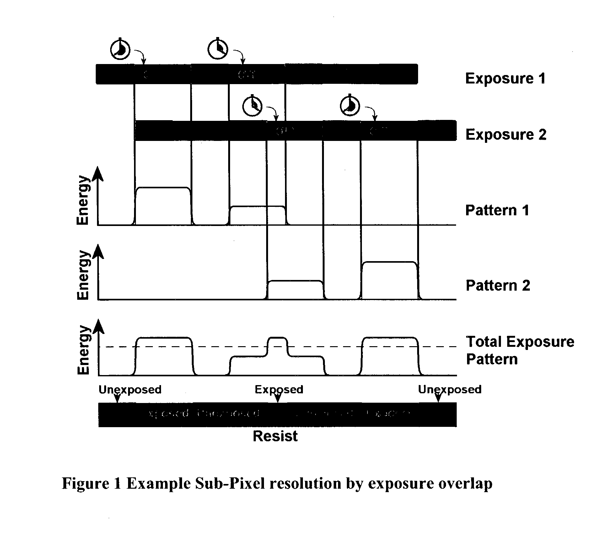
Advanced exposure techniques for programmable lithography
a lithography and programmable technology, applied in the field of programmable masks for exposing photoresists, can solve the problems of reducing the total energy deposited in the overlap region, arbitrary size, and variable feature placement and size,
- Summary
- Abstract
- Description
- Claims
- Application Information
AI Technical Summary
Benefits of technology
Problems solved by technology
Method used
Image

Examples
example preferred embodiment
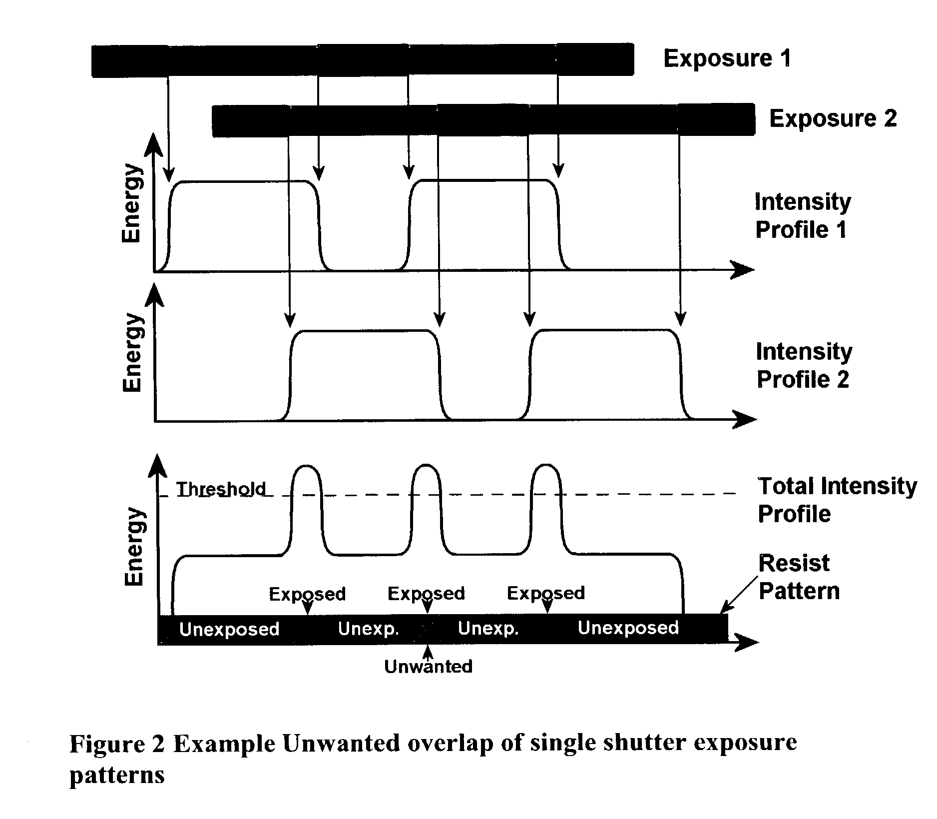
Photolithographic System Including Shutter Timing Control to Prevent Unwanted Features
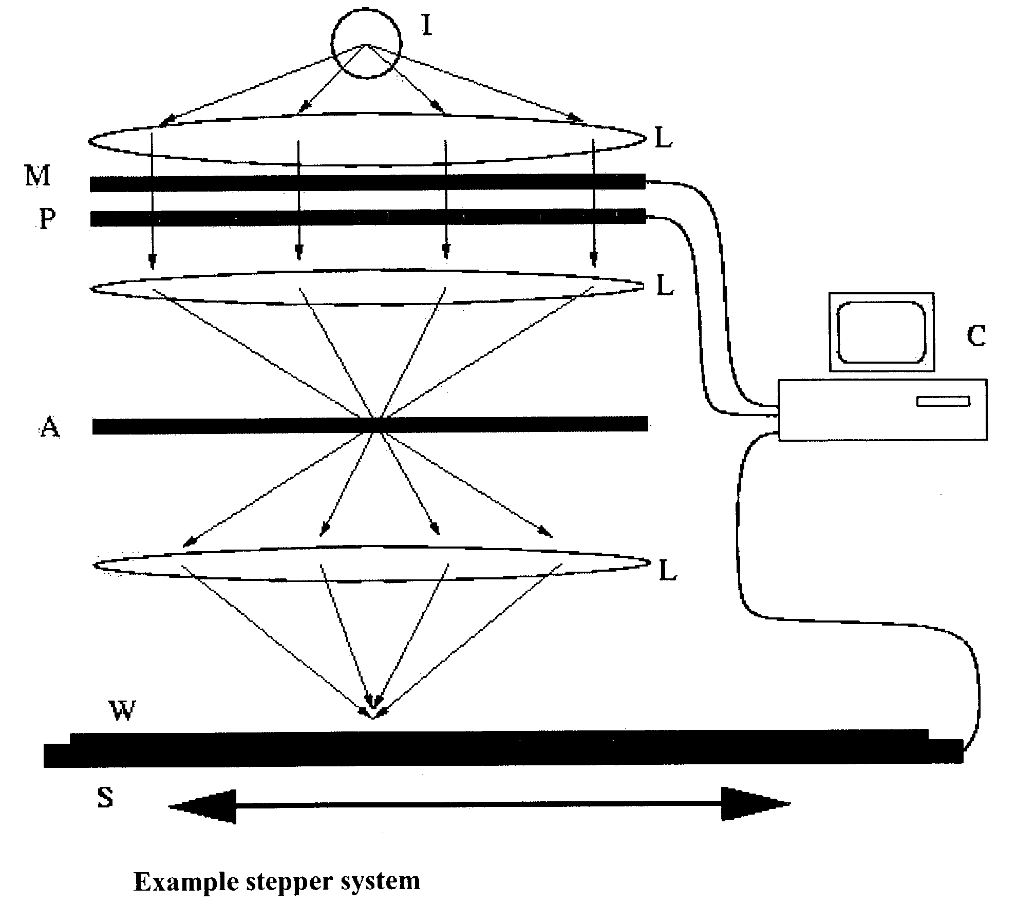
[0054]FIG. 4 shows an example mass production photolithographic system for exposing substrates such as but not limited to semiconductor wafers having photo-resist thereon. In the example embodiment shown in FIG. 4, a substrate such as a photo-resist coated wafer (“W”) is placed on a stage (“S”) which is used to move and position the substrate. A source of electromagnetic energy (“I”) such as, for example, visible light, x-rays, ultraviolet wavelengths, or other electromagnetic radiation wavelengths appropriate for the particular substrate and exposure processes being performed emits electromagnetic energy. In the example and illustrative embodiment, this electromagnetic energy is passed through a programmable mask (“M”) and then through an optical system of lenses and the like (“L”) that projects and demagnifies the image of the mask. The optical system may optionally include a programmable phase s...
example pattern
Decomposition Process
[0087]FIG. 9A shows an example pattern decomposition process provided by a presently preferred illustrative but non-limiting embodiment of the present invention. In the FIG. 9A example, a shutter-grid map matrix A is constructed (block 202) and inverted to obtain X as discussed above (block 204). A desired grid exposure vector G is then built based upon the X matrix (block 206). The shutter energy required to obtain vector E is found (block 208) and is checked for physical realizability (block 210). If the energy vector E is physically realizable (no negative in values), then the process is then complete (block 212). Otherwise, negative values in the vector E are set to 0 (block 214) and new grid exposure values are found (block 216) and tested against required limits (block 218). A modified target and exposure vector G′ is constructed (block 220) and used to determine a new required shutter energy vector E (block 208). This process may iterate as many times as ...
example implementation (
[0135]In order to implement an apodized imaging system for metrology, we can take one of several approaches. For example, we can apodize the imaging system or we can create an apodized projection system which projects a substantially sub-wavelength spot onto the wafer or mask being imaged, and the spot is scanned to image the whole object.
[0136]In the case of an apodized imaging system, we choose the apodizing function to create a narrow central distribution with a flat region on either side. The size of this flat region dictates the maximum size of the region on the object that can be imaged at any one time. The sensor used to detect the image (for example a CCD) need be no larger than the size of this flat region. In order to image the whole of the object the imaging system must be scanned relative to the object, unless the object is so small that it fits entirely within the flat region. One possible improvement is to implement the metrology system as a series of paralle...
PUM
| Property | Measurement | Unit |
|---|---|---|
| aperture radius | aaaaa | aaaaa |
| aperture radius | aaaaa | aaaaa |
| size | aaaaa | aaaaa |
Abstract
Description
Claims
Application Information