Check patentability & draft patents in minutes with Patsnap Eureka AI!

Built-in testing methodology in flash memory

Inactive Publication Date: 2006-05-23
STMICROELECTRONICS SRL
View PDF8 Cites 31 Cited by
  • Summary
  • Abstract
  • Description
  • Claims
  • Application Information

AI Technical Summary

Benefits of technology

[0010]It has been found that significant savings in terms of a reduced requisite of complexity of the testing hardware and of the software to implement an effective EWS flow by expanding the functions of the micro-controller normally embedded in a FLASH EPROM memory device and of the integrated test structures.
[0013]To do so, numerous architectural features will be illustrated in detail in the specific descriptions that will follow, moreover, the new architecture includes a “Column Test User Interface” that allows for a standardization of the testing and device debugging phases. The architecture of this invention provides for the execution of the above-listed routines internally without involving any external complex or expensive test equipment to control the test program. The processes are executed by the onboard micro-controllers (that may be reading either from an embedded ROM or from a GLOBAL CACHE purposely provided). Such a GLOBAL CACHE may be downloaded with the desired routine to a TUI block and provides a full test flexibility also at device debug level.
[0014]Managing test routines by an internal process allows the device architecture to be transparent from a tester point of view, by purposely creating a standard interface with a set of defined commands and instructions to be interpreted by the on board micro-controller and internally executed.
[0015]Advantages derivable through an implementation of the architecture of this invention include: Standardize TM protocol on different Flash Memory devices; Faster debug of new products to contribute positively to decrease time to market; Re-use of outdated test equipment, considering the case of testers with limits on frequency accuracy, memory space, CPU speed, advanced features, redundancy analysis; Extension of tester equipment life; Faster porting on different tester platforms—code development is almost standard and easily portable on different testers; Use of low-cost or parallel architecture testers; Cost saving on tester hardware and software accessories and options—i.e. buffer memory (BM), Error Catch RAM (ECR), Vector Memory (VM), pin electronics (p.e.), frequency range, bitmap tools.

Problems solved by technology

Developing and debugging the software of an EWS flow for a new device to be manufactured is a time consuming and relatively costly job.
Testing machines are also expensive.
Both the software and the testing hardware have a cost that is commensurate to the complexity and numerosity of tests that must be performed according to the EWS flow to achieve the acceptable reliability.

Method used


Image

  • Built-in testing methodology in flash memory
  • Built-in testing methodology in flash memory
  • Built-in testing methodology in flash memory

Examples


Embodiment Construction

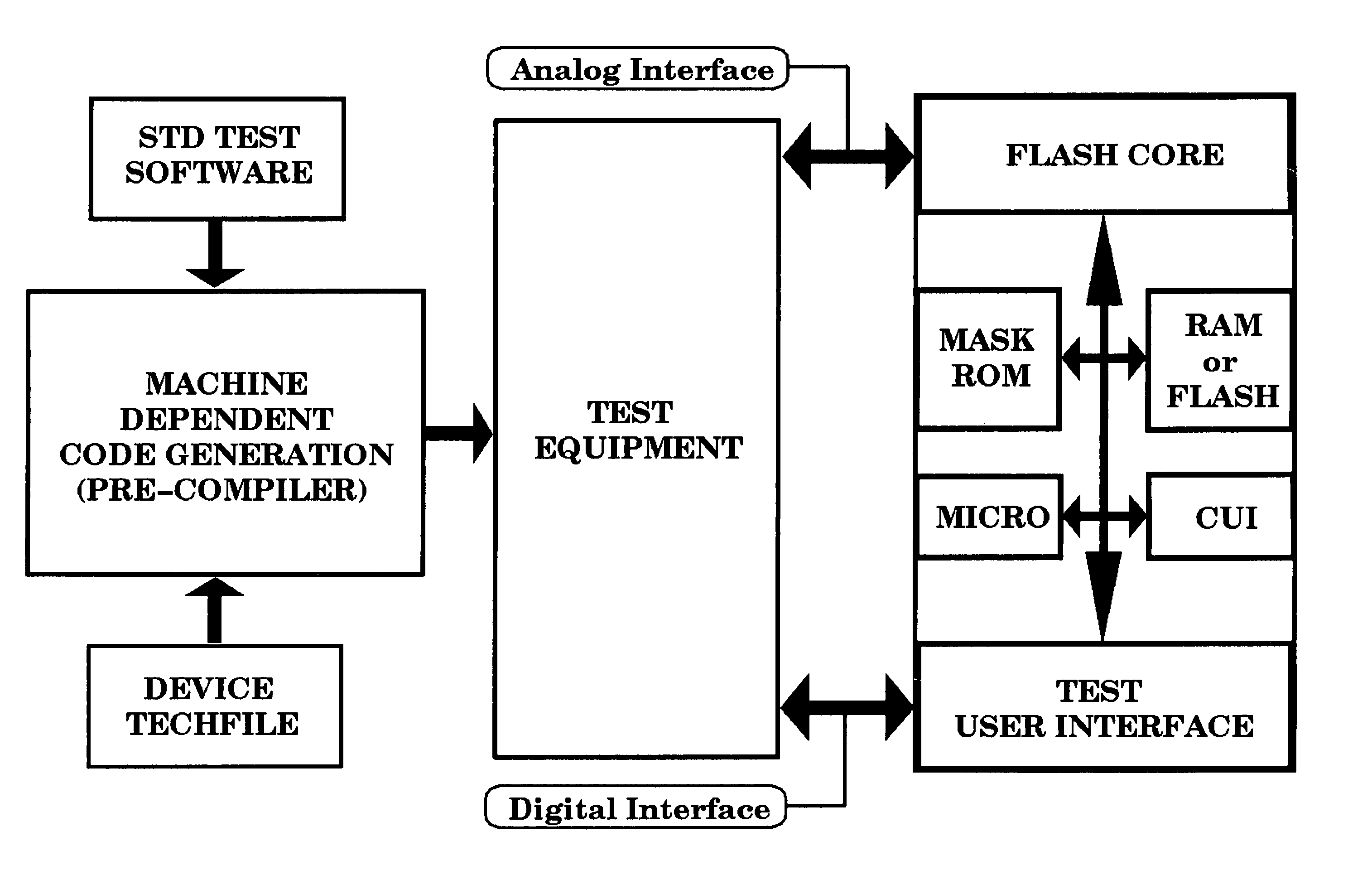
[0041]The built-in system according to the present invention is based on an architecture, a high level diagram of which is depicted in FIG. 2. The fundamental circuit blocks and their respective functions are as follows:

[0042]EXPECTED DATA GENERATION: generates the expected datum;

[0043]DATA COMPARISON: compares the expected datum with the datum read by the sense amplifier and writes the result of the comparison on the LOCAL_DATA_CACHE;

[0044]LOCAL DATA CACHE: it is composed of N registers, equal to the number of column redundancy resources available for each sector of the memory array, each of which is composed by M bit (where M coincides with the read parallelism of the SENSE BANK). A vector containing the information relatives to the bits on which a failure has occurred is stored in the register;

[0045]RESOURCE COUNTER: it contains an up / down counter, the purpose of which is to point to one of the register of the LOCAL DATA CACHE to one of the registers of the LOCAL ADDRESS CACHE an...


PUM


Abstract

An Electric Wafer Sort (EWS) flow is implemented by expanding the functions of the micro-controller embedded in a FLASH EPROM memory device and of the integrated test structures. Test routines are executed by the onboard micro-controllers (that may be reading either from an embedded ROM or from a GLOBAL CACHE provided) internally without involving any external complex or expensive test equipment to control the test program. The device architecture is transparent from a tester point of view, with a standard interface having a set of defined commands and instructions to be interpreted by the on board microcontroller and internally executed.

Description

FIELD OF THE INVENTION[0001]This invention relates in general to the fabrication of integrated digital devices and in particular to the techniques of quality testing, configuration, repair and validation of memory devices that are carried out at wafer level during the fabrication process.BACKGROUND OF THE INVENTION[0002]For enhancing quality standards and productivity in the semiconductor industry, not only implementation of improved technologies resulting from research and development efforts but also unrelated efforts in the areas of design, validation and engineering that may ensure a good test coverage in the shortest time are needed to meet time to market targets and reduce costs. The speeding up of the industrialization phase and optimizing test strategy for timely achieving validation and qualification of devices involves several factors such as the choice of the testing platform and of the level of test coverage, built-in self-tests, device settings and repair techniques. To...

Claims


Application Information

Patent Timeline
IPC IPC(8): G11C29/00G11C29/16
CPCG11C29/16G11C16/04G11C2029/0405G11C2029/0401
Inventor KUMAR, PROMODTOMAIUOLO, FRANCESCONICOSIA, PIERPAOLODE AMBROGGI, LUCA GIUSEPPEPIPITONE, FRANCESCO
Owner STMICROELECTRONICS SRL
Features
  • R&D
  • Intellectual Property
  • Life Sciences
  • Materials
  • Tech Scout
  • Unparalleled Data Quality
  • Higher Quality Content
  • 60% Fewer Hallucinations
Learn More