Method and structure for providing improved thermal conduction for silicon semiconductor devices

a technology of silicon semiconductor devices and thermal conduction structures, which is applied in the direction of semiconductor devices, semiconductor/solid-state device details, electrical apparatus, etc., can solve the problems of reducing the thermal conductivity of silicon semiconductor devices, increasing leakage current exponentially, and discharging heat to the 400, so as to achieve low electrical conductivity and high thermal conductivity

Inactive Publication Date: 2006-05-30
IBM CORP
View PDF20 Cites 63 Cited by
  • Summary
  • Abstract
  • Description
  • Claims
  • Application Information

AI Technical Summary

Benefits of technology

[0013]These and other objectives are realized by the present invention including a first silicon-on-insulator embodiment which comprises a plurality of thermal paths, formed after shallow trench and device fabrication steps are completed, which extend through the buried oxide and provide heat dissipation through to the underlying bulk silicon substrate. The thermal conduction path material is preferably diamond which has high thermal conductivity with low electrical conductivity. A second diamond trench cooling structure, formed after device fabrication has been completed, comprises diamond shallow trenches disposed between the devices and extending through the buried oxide layer. Similar diamond trench structures can be implemented when forming semiconductors in bulk silicon. An alternative diamond thermal cooling structure includes a diamond insulation layer deposited over the semiconductor devices. For transistors, yet another embodiment comprises diamond sidewalls formed along the gate walls in thermal contact with the device junctions to provide heat dissipation through the device junctions to underlying cooling structures. Diamond sidewalls may also be used for channeling heat from other semiconductor devices and from interconnect wiring disposed at the substrate surface. It is also proposed that the foregoing structures, and combinations of the foregoing structures, could be used in conjunction with other known cooling schemes such as the backside diamond cooling fins taught by the aforementioned Joshi, et al patent and patent application.

Problems solved by technology

Moreover, as device dimensions decrease, leakage current grows exponentially.
While SOI structures are advantageous for reduction of parasitic capacitance otherwise associated with bulk silicon CMOS devices, there are disadvantages to the isolation provided by the buried oxide layer.
With the isolation provided by the buried oxide, the devices cannot dissipate heat to the 400–600 micron silicon substrate, as efficiently as devices formed on bulk silicon had allowed, since the BOX is a thermal barrier.
A disadvantage to the former Joshi structure is that back-side cooling does nothing for dissipating heat away from the front-side-mounted devices.
A disadvantage to the latter Joshi front-side structure and method is that the trenches are formed prior to device fabrication.
As a result, the diamond in the trenches must be recessed and covered to protect it from the subsequent processing steps; thereby requiring numerous additional processing steps and resulting in an unusual structural profile.

Method used


Image

  • Method and structure for providing improved thermal conduction for silicon semiconductor devices
  • Method and structure for providing improved thermal conduction for silicon semiconductor devices
  • Method and structure for providing improved thermal conduction for silicon semiconductor devices

Examples


Embodiment Construction

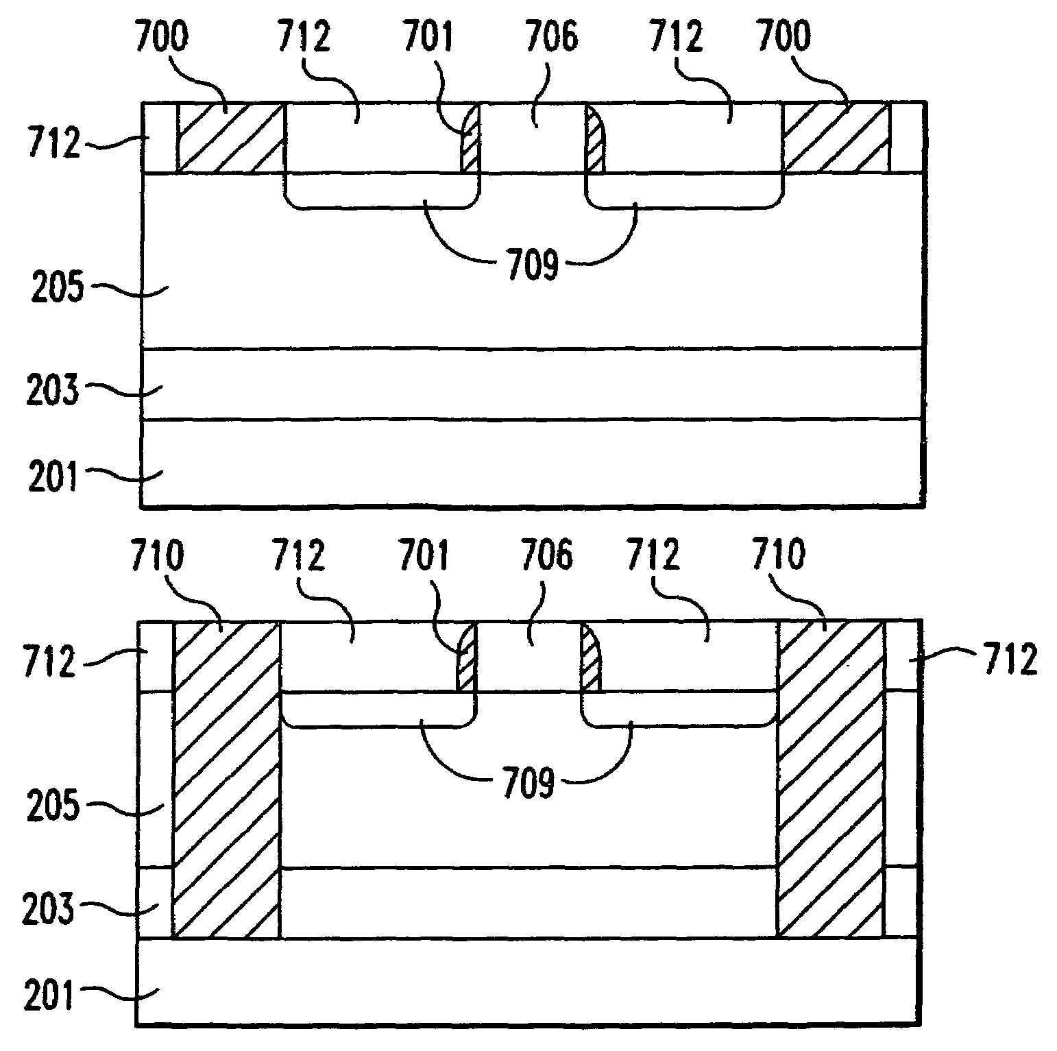
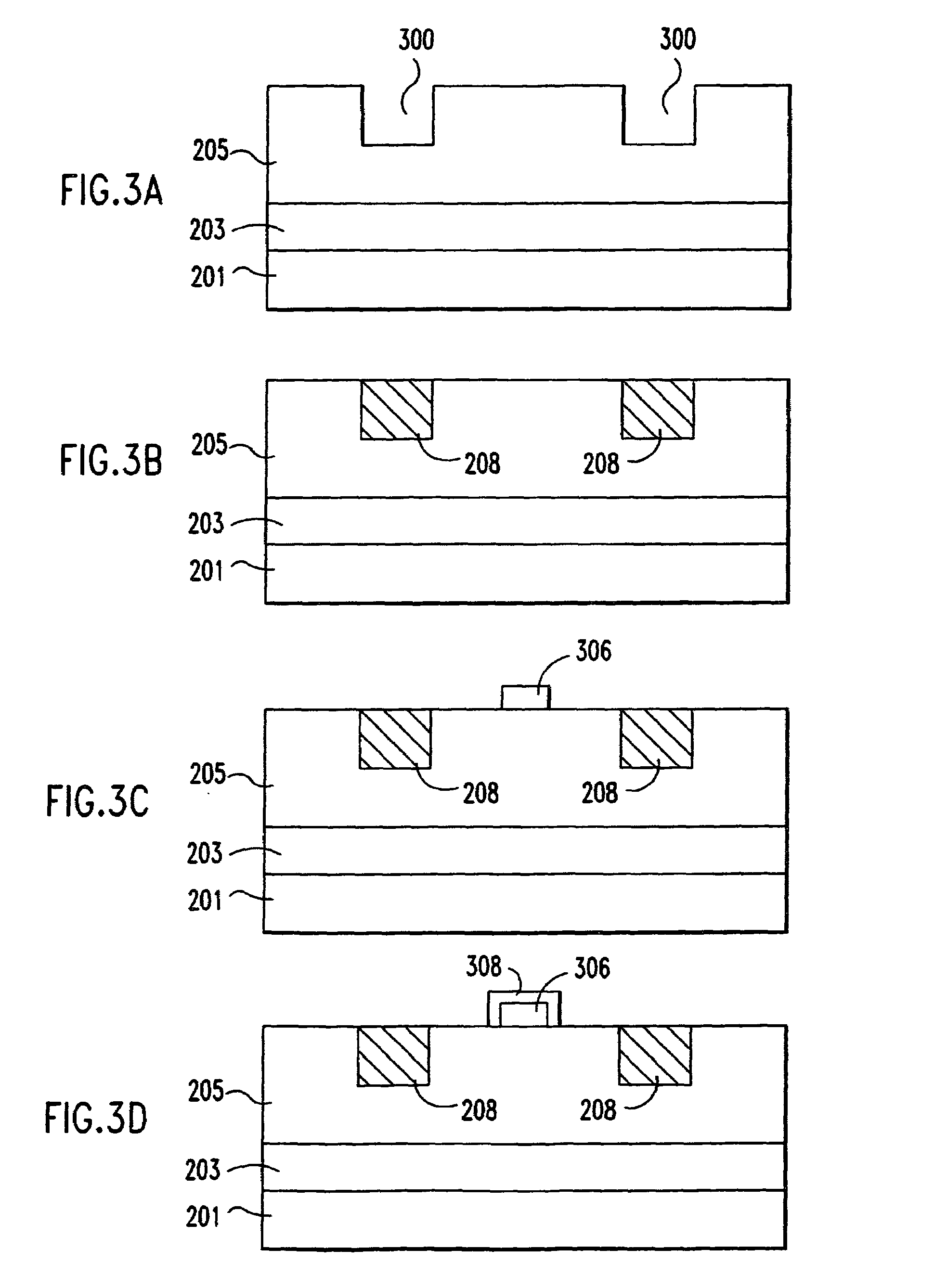
[0023]The present invention provides semiconductor cooling structures which are superior to those found in the prior art. The cooling structures include a first embodiment comprising thermal conduction paths formed in a silicon-on-insulator (SOI) structure having a buried oxide (BOX) layer, where the thermal conduction paths are formed between the shallow trench layers which isolate device and extend through the BOX layer to contact the underlying silicon. A second implementation of the invention provides for formation of diamond shallow trench regions between devices after device fabrication has been completed, either on an SOI or a bulk silicon structure. Under such an embodiment, more effective thermal conduction paths can be provided in the shallow trenches since the diamond would not require silicon nitride and oxide overlayers to protect it from subsequent thermal oxidation steps. Another embodiment includes a planar, thermally conductive insulation layer disposed over the com...


PUM

PropertyMeasurementUnit
thicknessaaaaaaaaaa
thicknessaaaaaaaaaa
thermal conductionaaaaaaaaaa

Abstract

Thermal cooling structures of diamond or diamond-like materials are provided for conducting heat away from semiconductor devices. A first silicon-on-insulator embodiment comprises a plurality of thermal paths, formed after shallow trench and device fabrication steps are completed, which extend through the buried oxide and provide heat dissipation through to the underlying bulk silicon substrate. The thermal conduction path material is preferably diamond which has high thermal conductivity with low electrical conductivity. A second diamond trench cooling structure, formed after device fabrication has been completed, comprises diamond shallow trenches disposed between the devices and extending through the buried oxide layer. An alternative diamond thermal cooling structure includes a diamond insulation layer deposited over the semiconductor devices in either an SOI or bulk silicon structure. Yet another embodiment comprises diamond sidewalls formed along the device walls in thermal contact with the device junctions to provide heat dissipation through the device junctions to underlying cooling structures. It is also proposed that the foregoing structures, and combinations of the foregoing structures, could be used in conjunction with other known cooling schemes.

Description

[0001]This is a division of application Ser. No. 09 / 362,399, filed Jul. 28, 1999 now U.S. Pat. No. 6,573,565.FIELD OF THE INVENTION[0002]This invention relates to semiconductor device cooling and, more particularly, to a method and structure for providing CVD diamond thermal conduction structures for semiconductor devices.BACKGROUND OF THE INVENTION[0003]Semiconductor chips require cooling to sustain reliability of circuits and interconnects formed on and in the semiconductor chips, to optimize circuit switching performance, and to suppress thermally generated noise in the circuits. An increased need for thermal cooling is seen for CMOS transistors, wherein high temperatures yield significantly larger leakage currents due to thermal generation of carriers. Moreover, as device dimensions decrease, leakage current grows exponentially.[0004]As a result, a myriad of cooling structures have been devised for incorporation into the semiconductor chip structure itself and for use with semic...

Claims


Application Information

Patent Timeline
Patent Type & Authority Patents(United States)
IPC IPC(8): H01L21/44H01L21/762H01L23/367H01L23/373H01L27/12
CPCH01L21/76264H01L23/3677H01L23/3732H01L27/1203H01L21/76283H01L2924/0002H01L2924/00
Inventor CLEVENGER, LAWRENCE A.HSU, LOUIS L.WANG, LI-KONGYUAN, TSORNG-DIH
Owner IBM CORP
Why Eureka
Try Eureka