Method for forming sublithographic features during the manufacture of a semiconductor device and a resulting in-process apparatus

a technology of semiconductor devices and features, applied in the field of semiconductor device manufacturing, can solve the problems of limiting the minimum feature size and optical lithography deficiency, and achieve the effect of narrowing the opening in the hard mask layer and reducing the feature siz

Inactive Publication Date: 2006-05-30
ROUND ROCK RES LLC
View PDF7 Cites 218 Cited by
  • Summary
  • Abstract
  • Description
  • Claims
  • Application Information

AI Technical Summary

Problems solved by technology

One limit to this goal is the deficiencies in optical lithography which restrict the minimum feature size.

Method used


Image

  • Method for forming sublithographic features during the manufacture of a semiconductor device and a resulting in-process apparatus
  • Method for forming sublithographic features during the manufacture of a semiconductor device and a resulting in-process apparatus
  • Method for forming sublithographic features during the manufacture of a semiconductor device and a resulting in-process apparatus

Examples


first embodiment

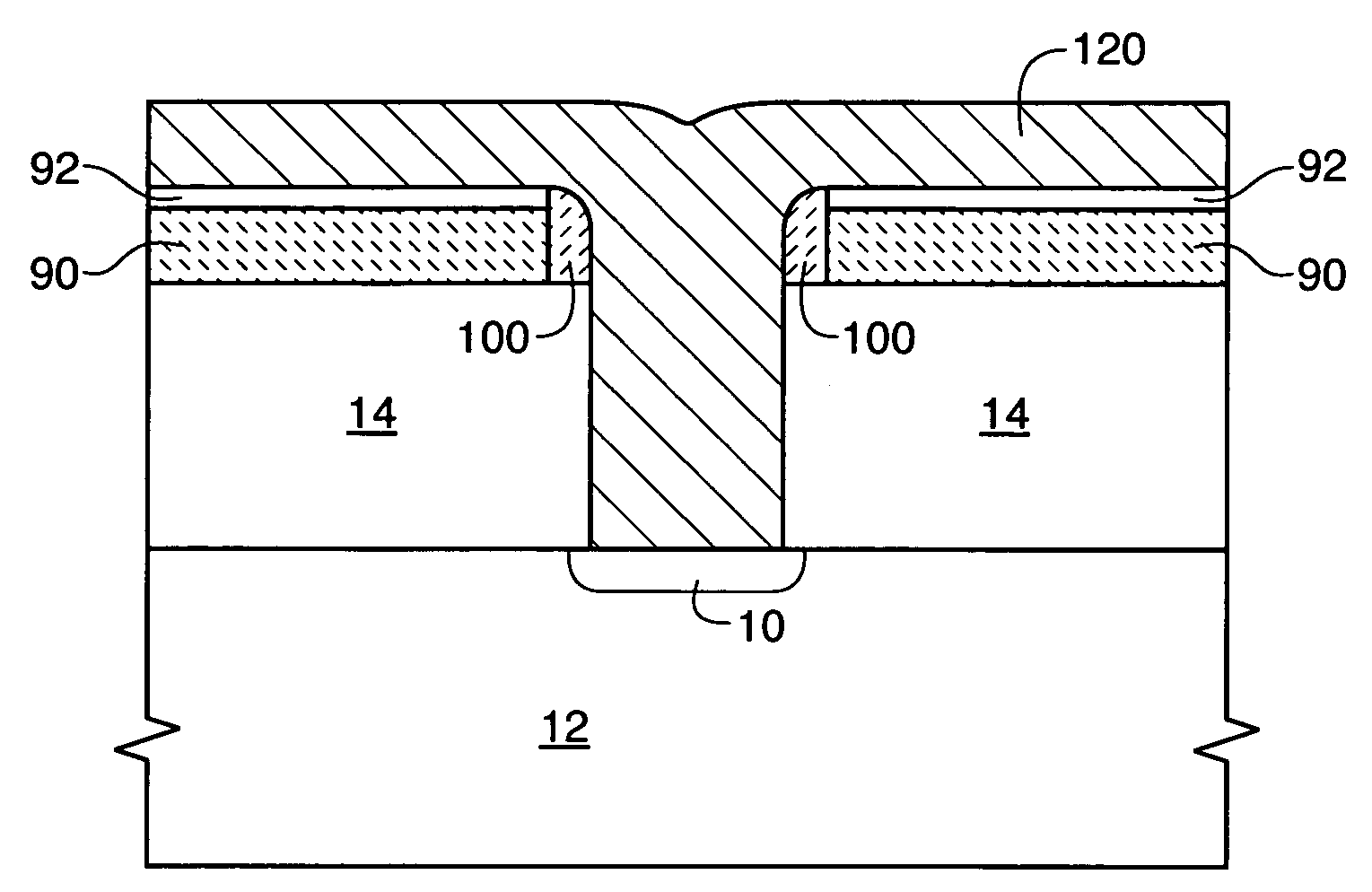
[0019]an inventive method for forming a feature in a semiconductor device is depicted in FIGS. 8–13, which specifically depict an embodiment of the invention used to form a digit line contact. It should be noted that various other structures may also be present in the device represented by the present FIGS. which are not immediately germane to the present invention and which, for simplicity of explanation, are not depicted.

[0020]FIG. 8 depicts a conductively-doped region 10 within a semiconductor wafer 12, and illustrates a planarized dielectric layer 14 such as one or more layers of borophosphosilicate glass (BPSG) and / or tetraethyl orthosilicate (TEOS) formed on the wafer 12. A hard mask layer 90 is formed over the dielectric, preferably from a material such as amorphous carbon (a-carbon). If required due to reflectance of hard mask 90, a dielectric antireflective coating (DARC) layer 92 is formed over the hard mask layer 90. A patterned photoresist layer 16 is formed on the DARC ...

second embodiment

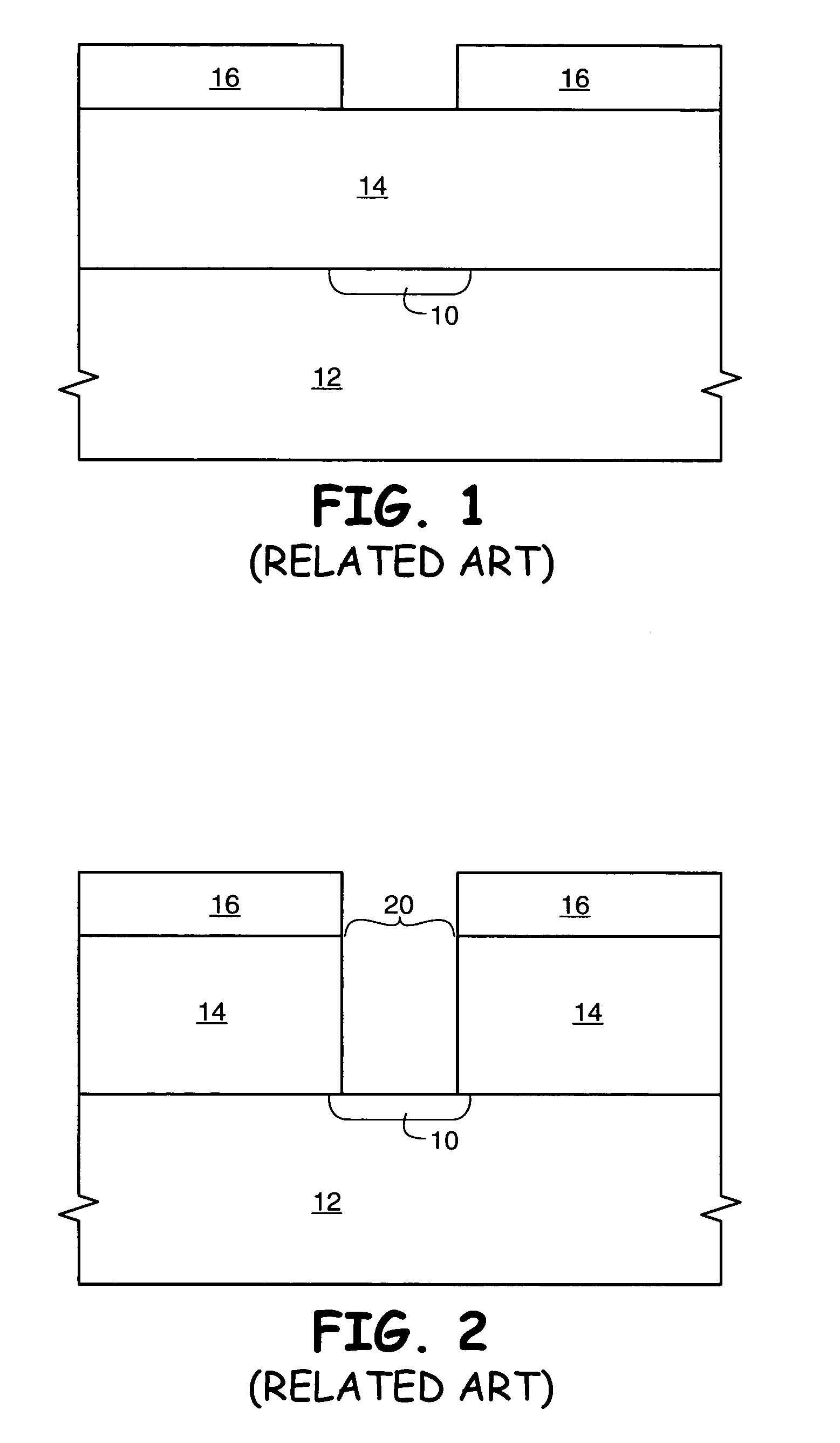
[0030]FIGS. 14–19 depict a second embodiment using the inventive method to define a plurality of transistor floating gates having minimal spacing between adjacent floating gates along a word line. FIG. 14 depicts a semiconductor wafer 12, gate oxide 56, floating gate layer 58, for example comprising polysilicon, capacitor dielectric 60, for example comprising a layer of silicon nitride interposed between two silicon dioxide layers (not individually illustrated), a hard mask layer 90 such as an a-carbon layer described above, and, if required, a DARC layer 92. The floating gate layer 58 at the point depicted in FIG. 14 comprises a plurality of parallel bands, one of which is depicted as element 58. These bands of floating gate material will be perpendicular to the word lines. A patterned photoresist layer 16 is formed which will define transistor floating gates. In this particular embodiment, the openings within photoresist layer 16 are formed at the minimum limits allowed by optical...


PUM

PropertyMeasurementUnit
thickaaaaaaaaaa
thickaaaaaaaaaa
temperatureaaaaaaaaaa

Abstract

A method for forming a semiconductor device comprises forming a layer to be etched, then forming a hard mask layer over the layer to be etched. The hard mask is etched to form an opening defined by first and second cross-sectional sidewalls in the hard mask layer. In one embodiment, the opening in the hard mask layer is formed at the minimum limits allowable by optical lithography. A conformal spacer layer is formed over the hard mask layer and on the sidewalls of the hard mask, then spacer etched to form first and second cross-sectional spacers along the first and second sidewalls in the patterned hard mask layer. The hard mask and spacers are preferably formed from amorphous carbon. The layer to be etched is etched using the hard mask layer and the spacers as a pattern, then the hard mask layer and spacers are removed.

Description

FIELD OF THE INVENTION[0001]This invention relates to the field of semiconductor manufacture and, more particularly, to a method for forming a device feature which is smaller than the lithography which defines it.BACKGROUND OF THE INVENTION[0002]During the manufacture of a semiconductor device, features are commonly patterned using optical lithography (photolithography). An exemplary photolithographic method and formation of a digit line contact is depicted in FIGS. 1–4. FIG. 1 depicts a conductively-doped diffusion region 10 within a semiconductor wafer 12, and a dielectric layer 14 such as borophosphosilicate glass (BPSG) formed over the wafer surface. A photoresist (resist) layer 16 is formed on the dielectric layer 14, then the photoresist layer is exposed and the exposed portion is removed to result in the structure of FIG. 1. The dielectric layer is etched using the resist 16 as a mask to form an opening 20 in the dielectric layer 14 to expose region 10 within semiconductor wa...

Claims


Application Information

Patent Timeline
Patent Type & Authority Patents(United States)
IPC IPC(8): H01L21/76H01L21/033H01L21/311H01L21/768
CPCH01L21/0337H01L21/76816H01L21/31144H01L21/0338
Inventor SANDHU, SUKESHSANDHU, GURTEJ S.
Owner ROUND ROCK RES LLC
Why Eureka
Try Eureka