Circuit device and method of manufacturing the same

a technology of circuit devices and die pads, which is applied in the direction of manufacturing tools, welding/cutting media/materials, and manufacturing tools, etc., can solve the problems of molten solder overflow from die pads, low-profile and lightweight, and inability to meet the requirements of small size, so as to achieve constant thickness of brazing materials 19 and increase bonding strength

Inactive Publication Date: 2006-05-30
SANYO ELECTRIC CO LTD +1
View PDF15 Cites 17 Cited by
  • Summary
  • Abstract
  • Description
  • Claims
  • Application Information

AI Technical Summary

Benefits of technology

[0029]First, the second plating film 14B is provided around the die pad 11 so as to enclose the semiconductor element 13, so that the brazing material 19 fixing the semiconductor element 13 can be prevented from overflowing in the present invention. Therefore, the brazing material 19 that has overflowed can be prevented from causing a short circuit between conductive patterns.
[0030]Second, in the step of mounting the semiconductor element 13, since the convex portion 14D is provided on both sides of the first plating film 14A where the semiconductor element 13 is mounted, the brazing material 19 can be caused to flow out from the part where the convex portion 14D is disposed. Therefore, the brazing material 19 can be caused to evenly flow out, and, as a result, the thickness of the brazing material 19 can be made constant. Furthermore, the semiconductor element 13 can be mounted in parallel with the conductive foil.
[0031]Third, since the second bonding pad 12B and the die pad 11 that are sealed with the insulating resin 16 are connected together through the wiring portion 20, the area of the side faces of the second bonding pad 12B and the die pad 11 can be increased. Therefore, an area where the bonding pad 12B, the die pad 11, and the insulating resin 16 are in contact with each other can be increased, and, as a result, the bonding strength among them can be increased. From this fact, the bonding pad 12 and the die pad 11 can be prevented from peeling off from the insulating resin 16.
[0032]Fourth, the first external electrode formed on the back surface of the die pad 11 is restricted in its position and size by the first opening 21B of the resist 18, and, likewise, the second external electrode 17B formed on the back surface of the bonding pad 12 is restricted in its position and size by the wettability of the back surface of the bonding pad 12. Therefore, the second external electrode 17B can be prevented from being deformed even when the opening 21 of the resist 18 deviates from a normal position.

Problems solved by technology

However, this package type semiconductor device 61 had the lead terminal 64 out of the resin layer 63, and was too large in total size to meet the requirements of small size, low-profile and lightweight.
Therefore, disadvantageously, molten solder overflows from the die pad 69, and the die pad 69 is short-circuited with other electrodes when the transistor T is placed on the molten solder.
This has brought about an increase in size of the whole of the device.

Method used


Image

  • Circuit device and method of manufacturing the same
  • Circuit device and method of manufacturing the same
  • Circuit device and method of manufacturing the same

Examples


first embodiment

(First Embodiment that Describes the Structure of a Circuit Device 10)

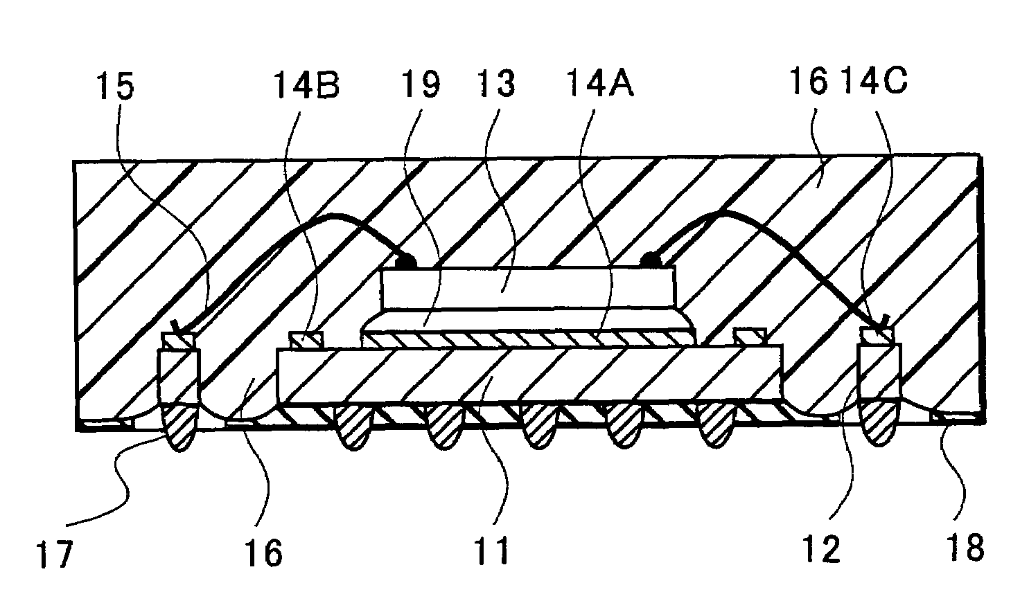
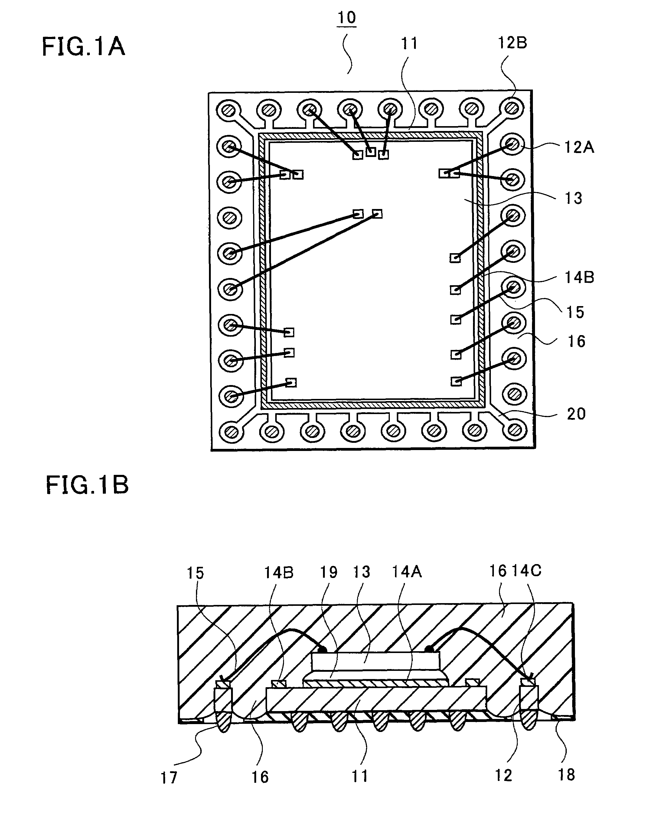
[0047]A description will be given mainly of the structure of the circuit device 10 of the present invention with reference to FIG. 1. FIG. 1(A) is a plan view of the circuit device 10, and FIG. 1(B) is a sectional view of the circuit device 10.

[0048]Referring to FIG. 1(A) and FIG. (B), the circuit device 10 is constructed as follows. That is, the circuit device 10 has a die pad 11 on which a semiconductor element 13 is mounted with a brazing material 19, a bonding pad 12 disposed in close vicinity to the die pad 11, and plating films formed on a surface of the die pad 11 and on a surface of the bonding pad 12, respectively, in which a second plating film 14B for preventing the brazing material 19 from overflowing is disposed around and apart from a first plating film 14A on which the semiconductor element 13 of the die pad 11 is mounted, and the brazing material 19 that has overflowed from the first plating film 1...

second embodiment

(Second Embodiment that Describes a Method of Manufacturing the Circuit Device 10)

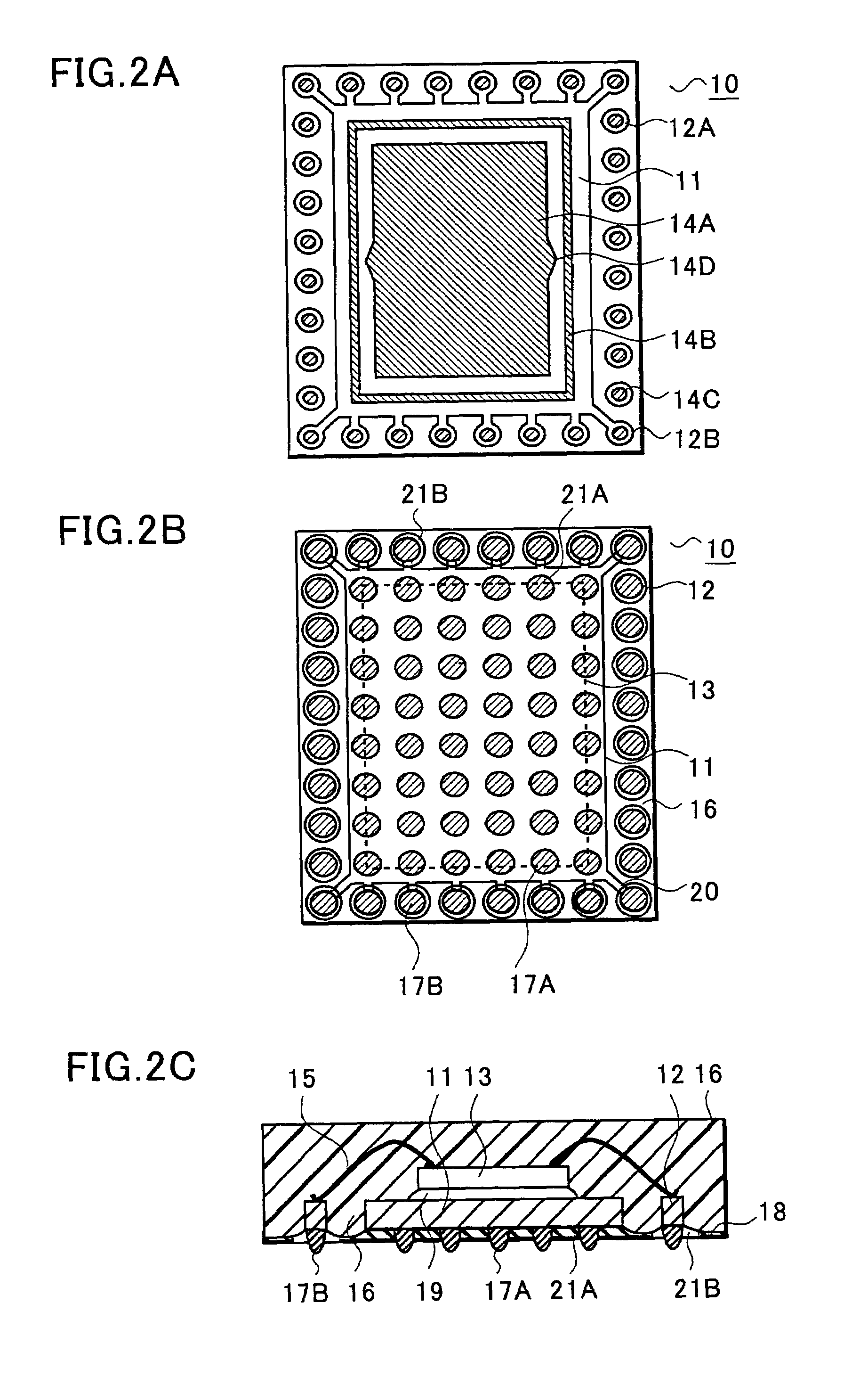
[0068]In this embodiment, a description will be given of a method of manufacturing the circuit device 10. The circuit device 10 is manufactured through the following steps in this embodiment. That is, the circuit device manufacturing method comprises a step of preparing a conductive foil 40; a step of forming die pads 11 and bonding pads 12 that constitute a plurality of circuit device portions 45 by forming a separation groove 16, which is smaller in thickness than the conductive foil 40, in the conductive foil 40; a step of forming a first plating film 14A on a surface of the die pad 11 corresponding to an area of a semiconductor element 13 to be fixed and, at the same time, forming a second plating film 14B so as to enclose the area thereof; a step of fixing the semiconductor element 13 onto the first plating film 14A with a brazing material 19; a step of performing wire bonding between the semicond...


PUM

PropertyMeasurementUnit
widthaaaaaaaaaa
semiconductoraaaaaaaaaa
widthaaaaaaaaaa

Abstract

The overflow of a brazing material (19) from a die pad (11) is prevented by forming a second plating film (14B) on the surface of the die pad (11). The second plating film (14B) is provided around the surface of the die pad 11 so as to enclose an area where a semiconductor element (13) is mounted. In a step of mounting the semiconductor element (13) on the die pad (11) with the brazing material (19), the brazing material (19) overflows from the first plating film (14A) when the semiconductor element (13) is mounted on the upper part of the molten brazing material. However, the second plating film (14B) functions as a blocking area by which the overflow of the brazing material is prevented. Therefore, a short circuit can be prevented from arising between the die pad (11) and the bonding pad (12) because of the brazing material that has spread.

Description

BACKGROUND OF THE INVENTION[0001]1. Field of the Invention[0002]The present invention relates to circuit devices capable of preventing a brazing material used to fix a semiconductor element from overflowing and relates to a method of manufacturing the circuit device.[0003]2. Description of the Related Art[0004]Conventionally, circuit devices to be set in an electronic apparatus have been required to be reduced in size, in thickness, and in weight, since the circuit devices are used for portable telephones, portable computers and so on. For example, a semiconductor device as a circuit device is typically a package type semiconductor device which is conventionally sealed by normal transfer molding. This semiconductor device is mounted on a printed circuit board PS as shown in FIG. 13.[0005]This package type semiconductor device 61 has a semiconductor chip 62 covered with a resin layer 63, with a lead terminal 64 for external connection derived from the side of this resin layer 63. How...

Claims


Application Information

Patent Timeline
Patent Type & Authority Patents(United States)
IPC IPC(8): H01L23/52H01L23/48H01L29/40B23K35/30C25D7/12H01L21/48H01L21/60H01L23/12H01L23/31H01L23/495H01L23/498H01L23/50
CPCC25D7/12H01L21/4832H01L23/3107H01L23/49582H01L23/498H01L23/49838H01L24/06H01L24/83H01L24/97H01L24/29H01L24/32H01L2224/05553H01L2224/05555H01L2224/05647H01L2224/291H01L2224/32225H01L2224/451H01L2224/48091H01L2224/48465H01L2224/73265H01L2224/8319H01L2224/83801H01L2224/92247H01L2224/97H01L2924/01004H01L2924/01005H01L2924/01013H01L2924/01029H01L2924/01033H01L2924/01047H01L2924/0105H01L2924/01059H01L2924/01078H01L2924/01079H01L2924/01082H01L2924/014H01L2924/14H01L2924/19041H01L2924/19043H01L2224/32245H01L2224/48247H01L24/45H01L24/48H01L2224/2919H01L2924/01006H01L2924/01024H01L2924/0665H01L2224/29101H01L2924/0132H01L2924/01028H01L2224/49171H01L2224/26175H01L2224/83H01L2224/85H01L2924/00014H01L2924/00H01L2924/01026H01L2224/85205H01L2924/00011H01L2924/12042H01L2224/04042H01L2924/181H01L2224/05554H01L24/49H01L2224/83205H01L2924/00012H01L21/60
Inventor TAKAHASHI, KOUJIKUSANO, KAZUHISASAKAMOTO, NORIAKI
Owner SANYO ELECTRIC CO LTD
Why Eureka
Try Eureka