

Electrical contacting device and method of making the same
a technology of electric contact and contact point, which is applied in the direction of circuit-breaking switches, relays, circuit-breaking switches for excess current, etc., can solve the problems of shortened production life becoming more serious, low-resistance metals have a relatively low melting point, and the reliability deterioration is more serious, so as to prevent a bridge forming, complete prevention of arc discharge, and the effect of reducing the induced voltage di/dt generated in opening and closing th
- Summary
- Abstract
- Description
- Claims
- Application Information
AI Technical Summary
Benefits of technology
Problems solved by technology
Method used
Image

Examples
first embodiment
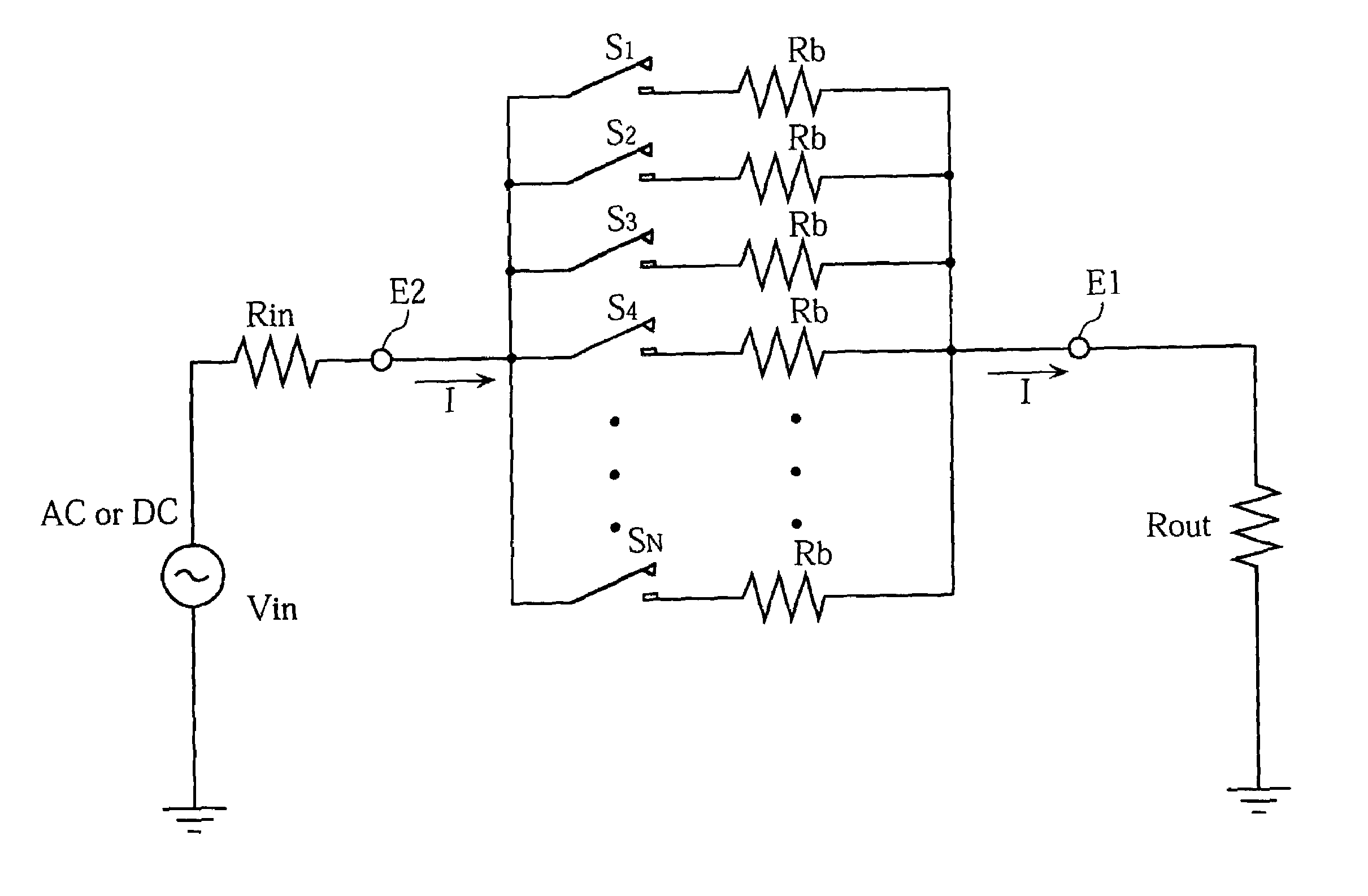
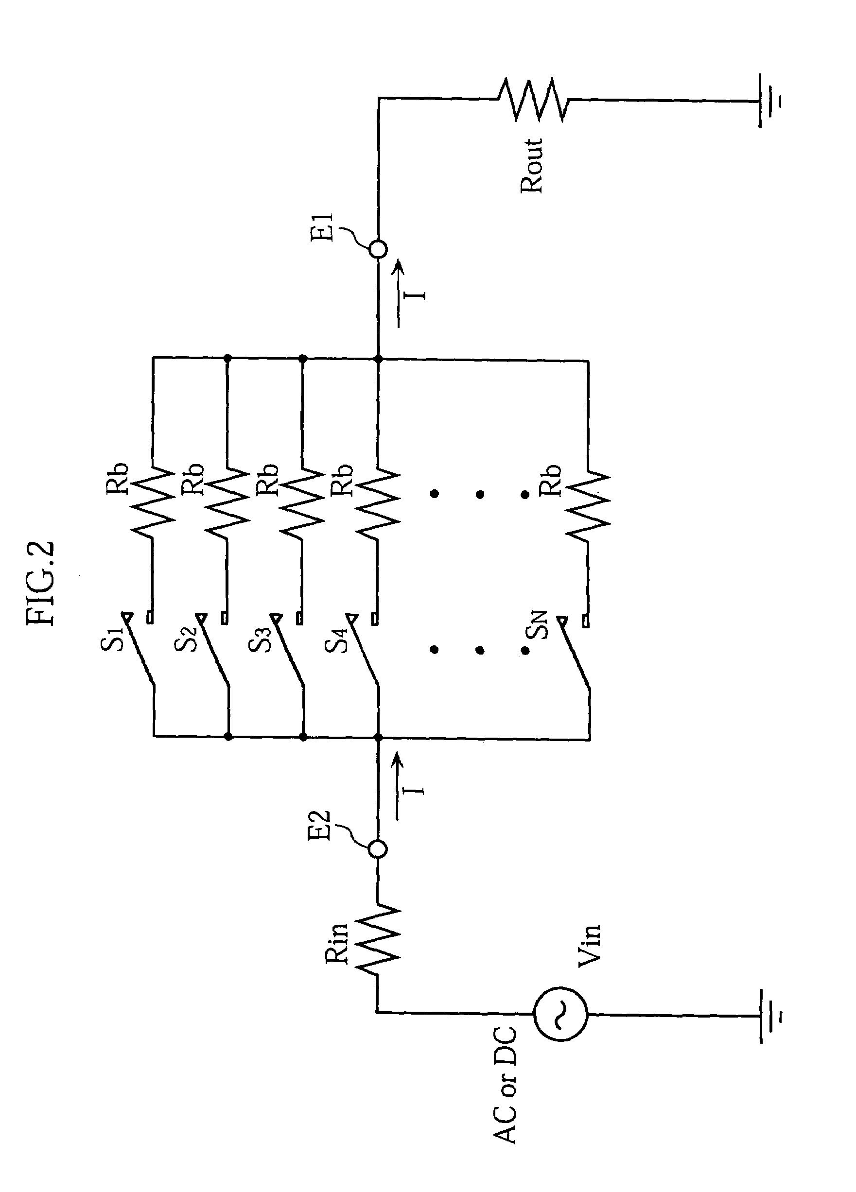
[0098]FIGS. 5 and 6 show an electrical contacting device X1 according to the present invention. The contacting device X1 includes a first contactor 10 and a second contactor 20. The first contactor 10 has a base 11, a plurality of projections 12, and a flat electrode 13. The base 11 is made of a suitable conductive material, for example, silicon. All the projections 12 are provided on one side of the base 11, each located at a prescribed position. The number of the projections 12 may be in a range of 100–100,000. Each projection 12 is in the form of a cone having a circular or polygonal base. The projections 12 are formed integral with the base 11 and made of the same material as the base 11. Each projection 12 is doped with impurities, as required, and a portion of the base 11 located under the projection 12 is also doped in the thickness direction of the base. Thus, the base 11 and the respective projections 12 are internally formed with resistive regions (resistors) having a pres...
third embodiment
[0121]FIG. 10 is a sectional view showing an electrical contacting device X3 according to the present invention. The unit X3 includes a first contactor 40 and a second contactor 20. The first contactor 40 includes a base 41, projections 42 and an electrode 43. It should be noted that in FIG. 10, the electrode 43 seems to have a plurality of separate parts, but actually the electrode 43 is a single, continuous element, as seen from FIG. 11.
[0122]The base 41 includes a rear portion 41a, a frame portion 41b, common fixing portions 41c, and beam portions 41d. As will be described later, these elements are integrally formed from a common material plate by a micro-machining technique. In the illustrated example, the frame portion 41b extends continuously along the four sides of the rectangular rear portion 41a (see FIG. 11).
[0123]As shown in FIG. 11, the common fixing portions 41c are arranged in parallel with each other on the rear portion 41a. Each of the fixing portions 41c is integral...
second embodiment
[0127]The function of the contacting device X3 is as follows. When the first contactor 40 is actuated to take the contact position, all the projections 42 are held in direct contact with the common electrode 22, whereby all the contacting points are closed. At this stage, the respective projections 42 are caused to press against the common electrode 22 with substantially the same pressing force. This feature is ascribed to the presence of the beams 41d. Specifically, even if the first contactor 40 and the second contactor 20 are oriented slightly askew (i.e., fail to be arranged in parallel), the beams 41d can sag to absorb extra pressing force acting between the projections 42 and the common electrode 22 held in mutual contact. Since the beams 41d have a cantilever structure, they are more flexible than the beams 31a of the Thus, the pressing force between the projections and the electrode is leveled off, whereby a proper contact condition is attained. In such a contact condition,...
PUM
 Abstract
Description
Claims
Application Information