Method of forming copper interconnects

a technology of copper interconnects and copper plates, applied in the direction of semiconductor devices, semiconductor/solid-state device details, electrical equipment, etc., can solve the problems of no production-worthy etching process for copper, increase in rc time delay, and failure to meet the requirements of etching process requirements

Inactive Publication Date: 2006-06-06
TAIWAN SEMICON MFG CO LTD
View PDF22 Cites 10 Cited by
  • Summary
  • Abstract
  • Description
  • Claims
  • Application Information

AI Technical Summary

Benefits of technology

[0009]In another embodiment of a method of forming copper interconnects for an integrated circuit, an interconnect pattern is patterned and etched in a low-k dielectric insulating layer. A dielectric diffusion barrier layer is conformally deposited over the etched insulating layer and a

Problems solved by technology

The use of copper as the interconnect material presents various fabrication problems.
First, there is currently no production-worthy etch process for copper.
As device sizes decrease to 0.1 μm and below, however, the main advantage of using low-resistance copper interconnects begins to be negated by the higher resistance met

Method used


Image

  • Method of forming copper interconnects
  • Method of forming copper interconnects
  • Method of forming copper interconnects

Examples


Embodiment Construction

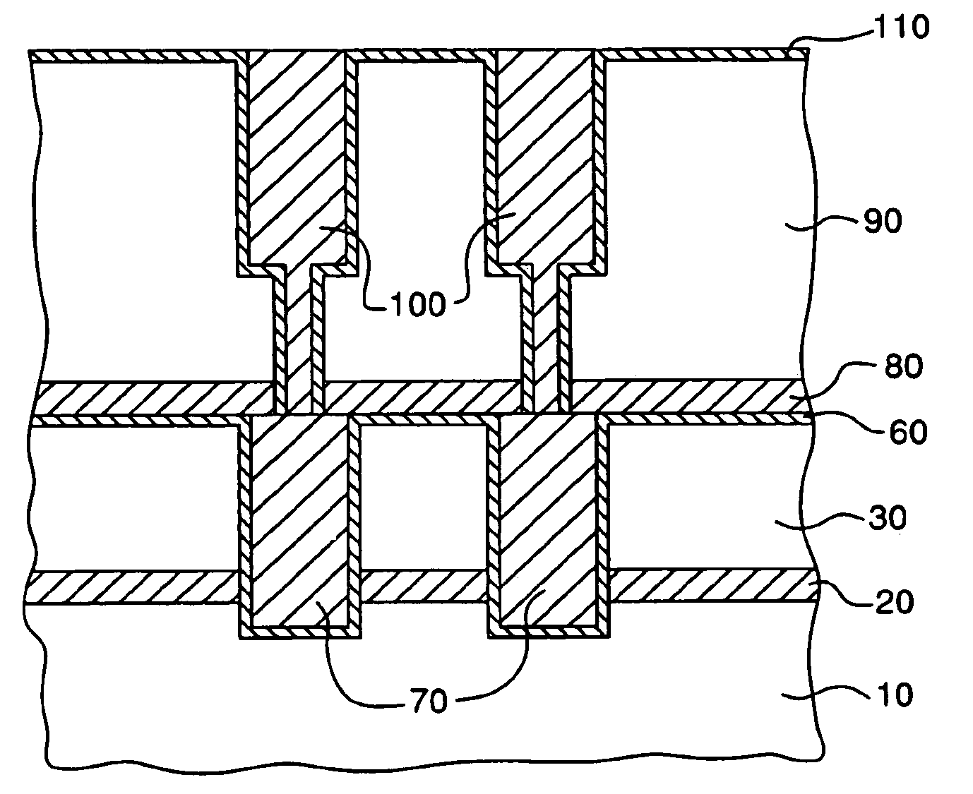
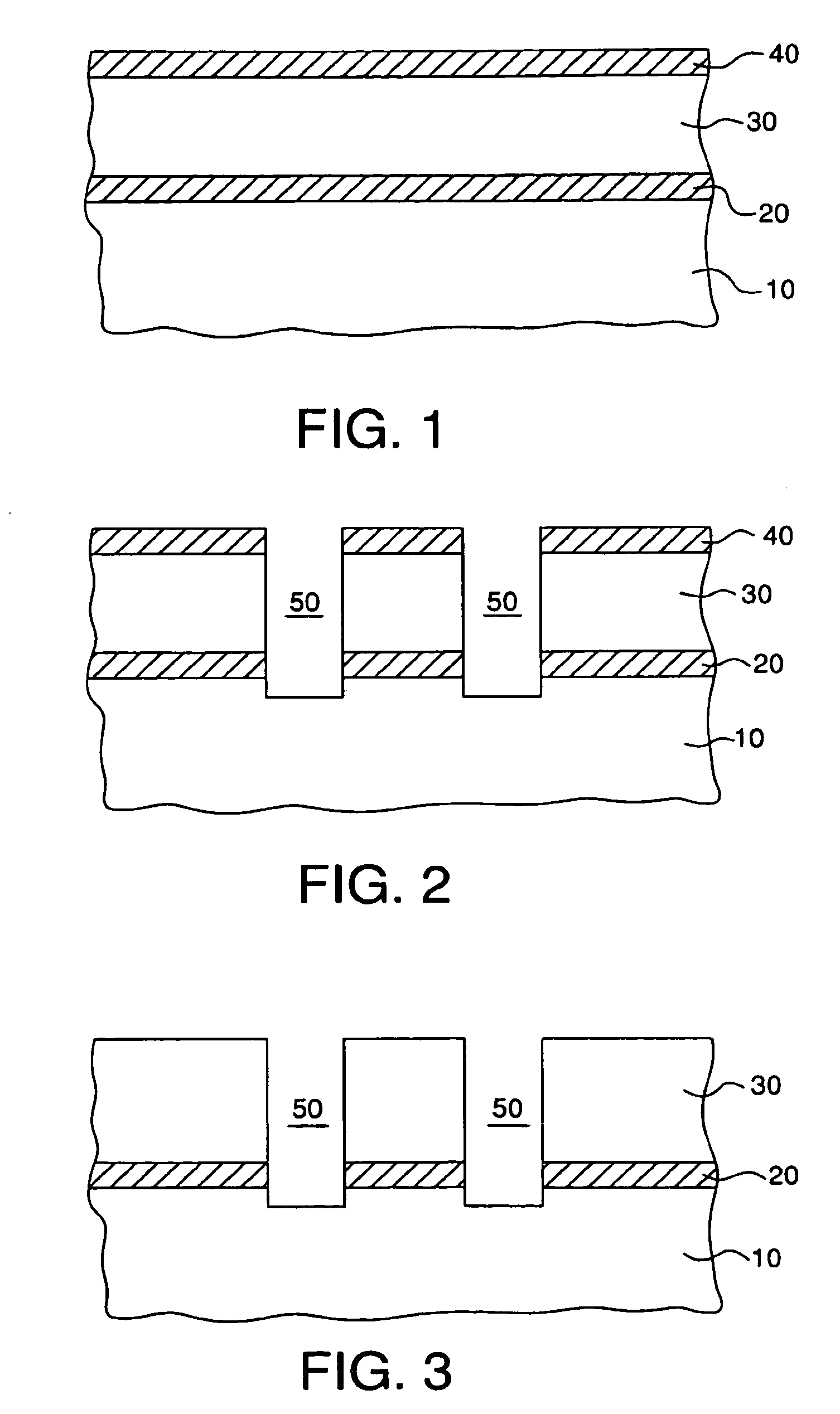
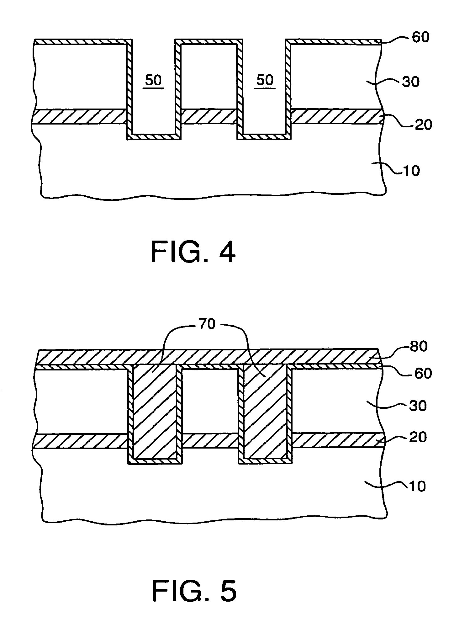
[0018]A damascene based method of forming a copper interconnect structure is described below in connection with FIGS. 1–6. It should be understood that the method described herein is equally applicable to both damascene and dual damascene fabrication techniques.

[0019]Referring first to FIG. 1, a cross-sectional view of a portion of the interconnect structure of a semiconductor device is provided. An etch stop layer 20 utilized in forming an interconnect pattern during the damascene process is formed over an insulating layer 10. In one embodiment, layer 10 includes an undoped silicate glass (USG), phosphosilicate glass (PSG) or boro-phosphosilicate glass (BPSG) material having a thickness greater than about 1.0 μm. Etch stop layer 20 typically includes SiN, SiC, SiCO, or SiCN deposited to a thickness between about 200–500 Å, and preferably about 400 Å. An inter-metal dielectric (IMD) layer 30 is deposited over the etch stop layer 20. IMD layer 30 may include SiO2 or a low-k dielectri...


PUM


Abstract

A method of forming copper interconnects for an integrated circuit is provided. An antireflective coating layer is formed over an insulating layer formed over a semiconductor substrate. An interconnect pattern is patterned and etched into said insulating layer. A diffusion barrier layer is then conformally deposited in a deposition chamber along the etched interconnect pattern, wherein the antireflective coating is removed in said chamber before deposition of the barrier layer. Copper interconnects are then formed in the interconnect pattern etched in the insulating layer.

Description

FIELD OF THE INVENTION[0001]The present invention relates to semiconductor fabrication techniques and structures, and more particularly to copper interconnects and methods of forming the same.BACKGROUND OF THE INVENTION[0002]Integrated circuits formed on semiconductor substrates typically include several metal layers that electrically interconnect the devices formed therein. The different metal layers are separated by insulating layers known as interlevel (or interlayer) dielectric layers (ILD) that have etched via holes (also known as vias) therein to connect devices or active regions from one layer of metal to the next.[0003]Copper (Cu) interconnects are increasingly used for high density devices because of copper's improved conductivity relative to conventional materials such as aluminum (Al). The use of copper as the interconnect material presents various fabrication problems. First, there is currently no production-worthy etch process for copper. The damascene and dual damascen...

Claims


Application Information

Patent Timeline
IPC IPC(8): H01L21/4763H01L21/768H01L23/522H01L23/532
CPCH01L21/76829H01L21/76831H01L21/76832H01L23/53295H01L21/7684H01L23/5226H01L23/53238H01L21/76834H01L21/76807H01L2924/0002H01L2924/00
Inventor WU, ZHEN-CHENGLU, YUNG-CHENGCHEN, YING-TSUNGJANG, SYUN-MING
Owner TAIWAN SEMICON MFG CO LTD
Why Eureka
Try Eureka