Dielectric materials

a technology of dielectric materials and dielectric materials, which is applied in the direction of inorganic insulators, crystal growth processes, condensed vapors, etc., can solve the problem of relatively high spatial anisotropy of alloy forms, and achieve the effects of preventing mobility decline, high spatial anisotropy, and improving thermodynamic stability

Inactive Publication Date: 2006-06-06
IBM CORP
View PDF7 Cites 76 Cited by
  • Summary
  • Abstract
  • Description
  • Claims
  • Application Information

AI Technical Summary

Benefits of technology

[0005]In accordance with the present invention, there is now provided an article of manufacture comprising a substrate and a layer of N(x)Y(1−x)AlO3 on the substrate where x is a molar fraction greater than zero and less than one, and N is an element selected from La, Ce, Pr, Nd, Pm, Sm, Eu, Gd, Tb, Dy, Ho, Er, Tm, Yb, and Lu. In preferred embodiments of the present invention, N is La. The layer preferably has a rhombohedral perovskite structure. In particularly preferred embodiments of the present invention, the layer has an average dielectric constant value between 15 and 35. The molar fraction x is preferably greater than 0.07. However, in particularly preferred embodiments of the present invention, x is less than 0.4. In some applications of the present invention, an electrode may be electrically isolated from the substrate by the layer. Examples of such applications include electronic devices such as field effect transistors in which

Problems solved by technology

Also, such forms of this alloy have

Method used


Image

  • Dielectric materials
  • Dielectric materials
  • Dielectric materials

Examples


Embodiment Construction

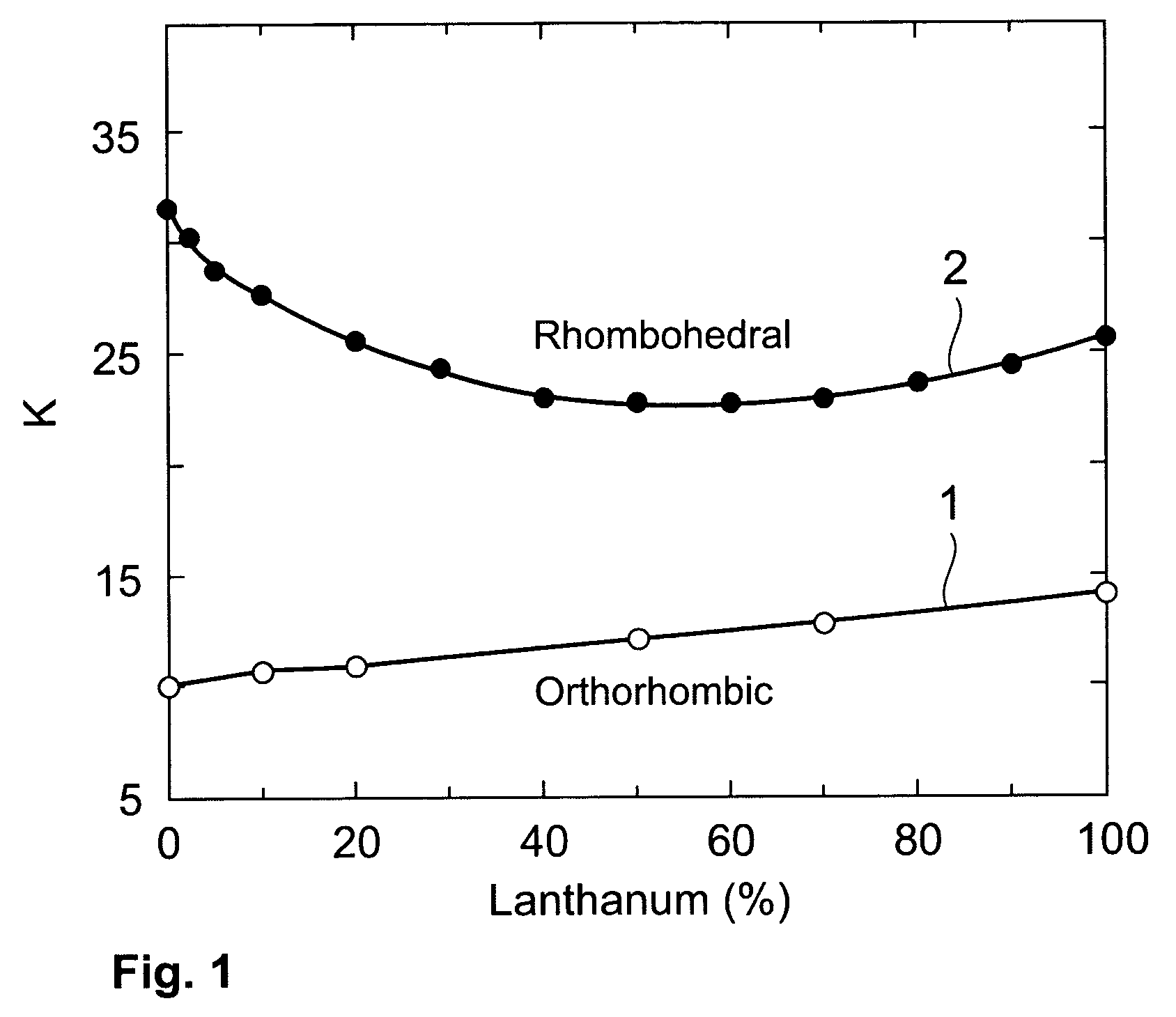
[0014]Experiments indicate that a stoichiometric alloy of Al2O3 and Y2O3 produces a crystalline solid solution YAlO3 (YAP) with an orthorhombic perovskite structure and a K value of around 15. YAlO3 is probably isotropic. In addition, Y2O3 / Si(1 0 0) interfaces have good electrical properties. By contrast, a stoichiometric alloy of Al2O3 and La2O3 produces a crystalline solid solution LaAlO3 (LAR) with a rhombohedral perovskite structure and a K value of around 26. LaAlO3 is probably highly anisotropic. However, La2O3 / Si(1 0 0) interfaces do not have good electrical properties. Despite this, we have found that alloys of YAlO3 and LaAlO3 have surprisingly desirable dielectric qualities. These qualities will now be described in detail.

[0015]Referring to FIG. 1, curve 1 demonstrates the theoretical average K value of La(x)Y(1−x)AlO3 in orthorhombic perovskite structure as a function of La concentration. Curve 2 demonstrates the theoretical K value of La(x)Y(1−x)AlO3 in rhombohedral pero...


PUM

PropertyMeasurementUnit
Fractionaaaaaaaaaa
Structureaaaaaaaaaa
Dielectric constantaaaaaaaaaa

Abstract

An article of manufacture comprises a substrate and a layer of N(x)Y(1−x)AlO3 on the substrate where x is a molar fraction greater than zero and less than one, and N is an element selected from La, Ce, Pr, Nd, Pm, Sm, Eu, Gd, Tb, Dy, Ho, Er, Tm, Yb, and Lu. The article may be an electronic device further comprising an electrode electrically isolated from the substrate by the layer. In particular, the dielectric properties of the layer are such that the layer is especially although by no means exclusively useful for electrically isolating gate electrodes in field effect transistor devices. The layer may be formed on the substrate via molecular beam epitaxy.

Description

FIELD OF THE INVENTION[0001]The present invention generally relates to dielectric materials and particularly relates to dielectric materials for semiconductor switch devices.BACKGROUND OF THE INVENTION[0002]Conventional semiconductor switch devices for very large scale integration (VLSI) applications include complementary metal oxide semiconductor (CMOS) switches. A CMOS switch typically comprises a field effect transistor having a conduction channel extending in a silicon substrate between a source electrode and a drain electrode. A gate electrode is disposed on the substrate between the source and drain. Conventionally, the gate electrode is insulated from the channel by a gate dielectric layer of silicon dioxide. In operation, the flow of current through the channel between the source and drain is controlled by application of voltage to the gate.[0003]To date, the performance of microprocessors based on CMOS technology has increased with time in a substantially exponential fashio...

Claims


Application Information

Patent Timeline
IPC IPC(8): H01L29/76C04B35/44C23C14/08C30B23/02H01B3/12H01L21/28H01L21/316H01L21/822H01L27/04H01L29/51H01L29/78
CPCC23C14/08C30B23/02H01L21/28167H01L21/31604C30B29/22H01L29/517H01L21/31616H01L21/02197H01L21/02269
Inventor ANDREONI, WANDACURIONI, ALESSANDROSHEVLIN, STEPHEN A.
Owner IBM CORP
Why Eureka
Try Eureka