Pulse output circuit, shift register and display device

a technology of shift register and output circuit, which is applied in logic circuit coupling/interface arrangement, digital storage, instruments, etc., can solve the problems of keeping the manufacturing cost of the display device down sufficiently, and achieve the effect of light weight, low price and sufficient manufacturing cost of the display devi

Inactive Publication Date: 2006-06-06
SEMICON ENERGY LAB CO LTD
View PDF53 Cites 114 Cited by
  • Summary
  • Abstract
  • Description
  • Claims
  • Application Information

AI Technical Summary

Benefits of technology

[0012]Demand for a display device using liquid crystal or spontaneous luminous elements is rapidly increasing as a mobile electronic apparatus is downsized and lightened in weight. It is difficult, however, to keep a manufacturing cost of the display device down sufficiently in view of a yield. It is easily forecasted that a future demand would more rapidly increase, and therefore, supply of a display device at a low price is desired.
[0013]A general method for forming a drive circuit on an insulating material is to perform exposure and etching of a pattern such as an activation layer and a wiring by means of plural photo-masks to form the circuit. The number of processes in manufacturing is ideally as few as possible since it directly influences a manufacturing cost. When the drive circuit conventionally comprising a CMOS circuit can be formed only by means of conductive TFTs, which are either one of the N-channel type or the P-channel type, a part of an ion-doping process can be omitted as well as the number of photo-masks can be reduced.
[0022]In view of the above problems, a purpose of the invention is to provide a pulse output circuit and a shift register capable of manufacturing at a low cost by using only single conductive TFTs to reduce manufacturing processes and capable of obtaining an output without amplitude attenuation.
[0024]In order to overcome the above, the following measures are taken in the invention. As shown in FIG. 10B, a capacity means 1003 is provided between the gate and the source of the N type of TFT 1001. When the potential of the output node is raised up at the time that the gate electrode of the N type of TFT 1001 is in a floating state with certain potential, the potential of the gate electrode of the N type of TFT 1001 is also raised up in accordance with a rising amount of the potential of the output node due to capacity combination by the capacity means 1003. It is possible to make the potential of the gate electrode of the N type of TFT 1001 higher than VDD (more accurately, higher than VDD+VthN) by using the above effect. Therefore, it is possible to rise up the potential of the output node to VDD sufficiently.

Problems solved by technology

It is difficult, however, to keep a manufacturing cost of the display device down sufficiently in view of a yield.
The number of processes in manufacturing is ideally as few as possible since it directly influences a manufacturing cost.

Method used


Image

  • Pulse output circuit, shift register and display device
  • Pulse output circuit, shift register and display device
  • Pulse output circuit, shift register and display device

Examples


embodiment mode 1

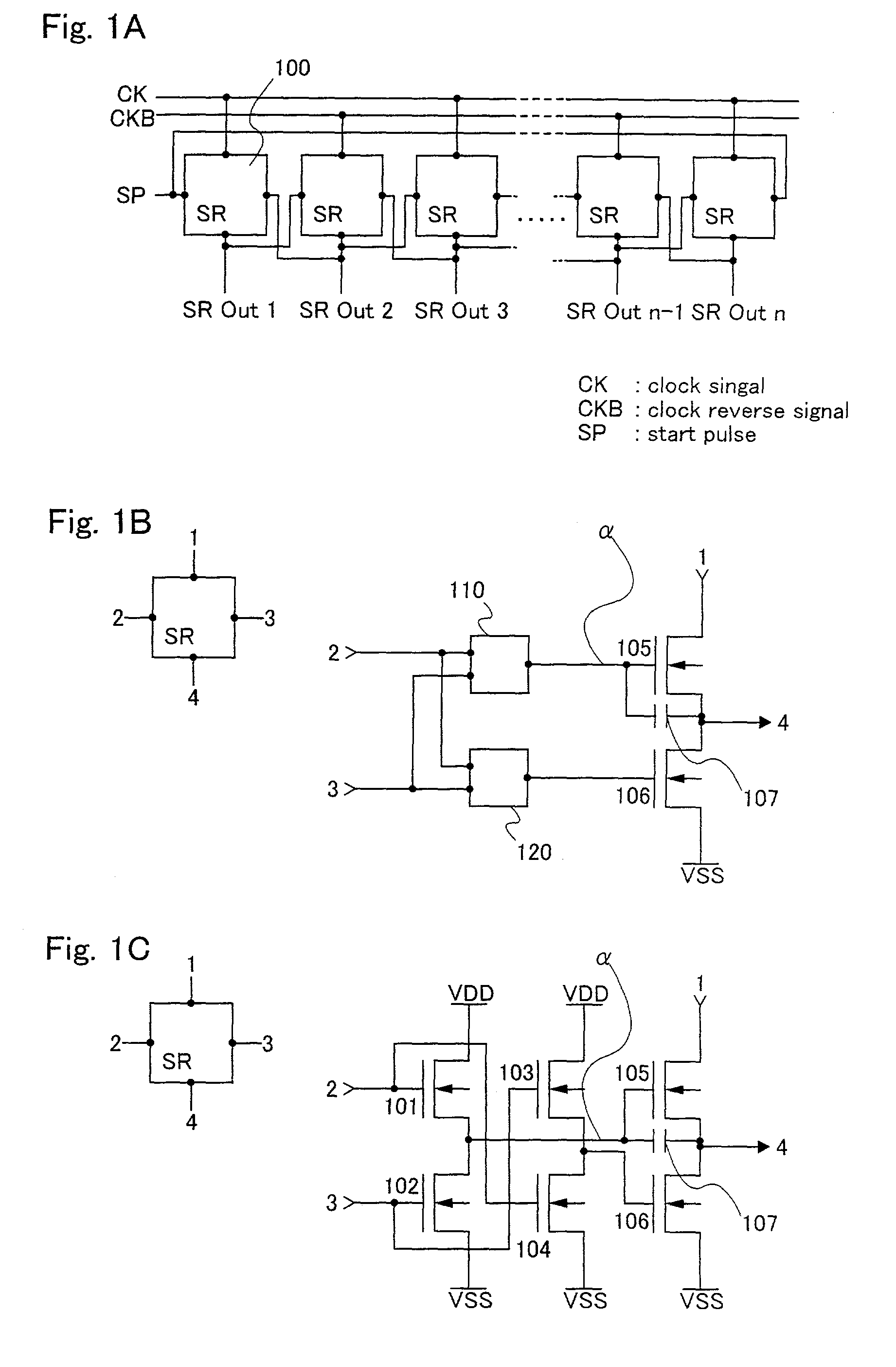
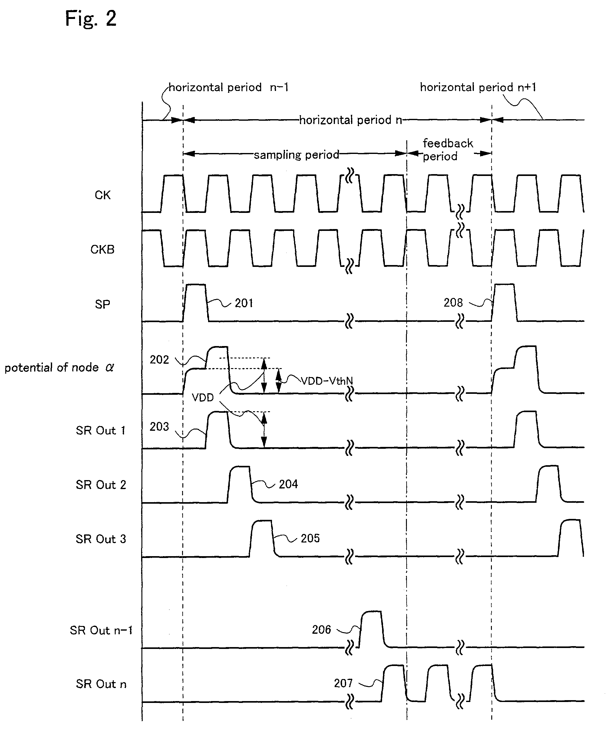
[0219]FIG. 1 illustrates a shift register to which a bootstrap manner is applied, which is in a mode of a pulse output circuit according to the invention. In a block diagram shown in FIG. 1A, a block shown by 100 is a pulse output circuit for outputting one stage of sampling pulses. A shift register shown in FIG. 1A comprises n stages of pulse output circuits. A clock signal (referred to as a CK, hereinafter), a clock reverse signal (referred to as a CKB, hereinafter) and a start pulse (referred to as an SP, hereinafter) are inputted to the shift register. FIG. 1B illustrates a detailed circuit structure of the block 100. In FIG. 1B, a block 110 is a first amplitude compensation circuit and a block 120 is a second amplitude compensation circuit. FIG. 1C illustrates a further detailed circuit structure. In FIG. 1C, the first amplitude compensation circuit 110 comprises a TFT 101 connected to power supply VDD and a TFT 102 connected to power supply VSS, while the second amplitude comp...

embodiment mode 2

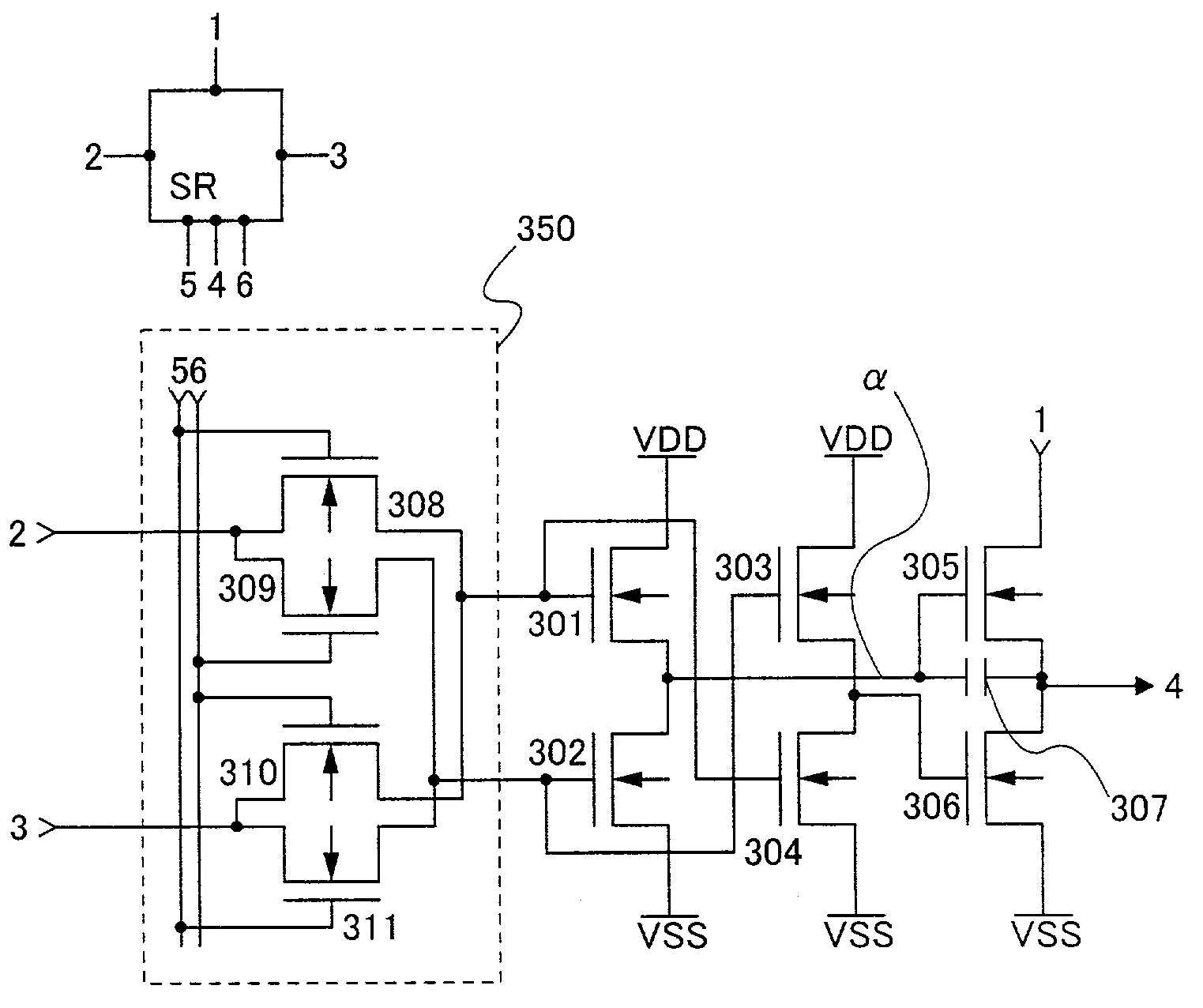
[0228]FIGS. 3A and 3B illustrate an example that a shift register shown in the present embodiment mode of the invention is added with a scan direction reverse function. In FIG. 3A, a scan direction switch signal (LR) and a scan direction switch back signal (LRB) are added thereto comparing with the circuit shown in FIG. 1A.

[0229]FIG. 3B illustrates a detailed structure of one stage of a pulse output circuit shown by a block 300 in FIG. 3A. A body of the pulse output circuit comprising TFTs 301 to 306 and a capacity means 307 is same as that of FIG. 1B, while a scan direction switch circuit shown by a dotted line frame 350 is provided between the second and third input signal lines (2) and (3) and the body of the pulse output circuit. The scan direction switch circuit in this embodiment mode comprises TFTs 308 to 311 and functions as an analog switch.

[0230]Gate electrodes of the TFTs 301 and 304 are connected to the second input signal line (2) through the TFT 308 and to the third in...

embodiment 1

[0235]An example of producing a display device by means of single conductive TFTs is described in this embodiment.

[0236]The substrate having the pixel TFT and the driver circuit may be manufactured in accordance with a known method, for example, as disclosed in U.S. Pat. No. 5,889,291 issued to Koyama et al. Also, it is possible to crystallize a semiconductor film for an active layer of the TFTs by utilizing a metal element for promoting crystallization although other known methods can be used for crystallization. Such a method of using the metal element is disclosed, for example, in U.S. Pat. No. 5,643,826 issued to Ohtani et al. The entire disclosures of these U.S. Pat. Nos. 5,889,291 and 5,643,826 are incorporated herein by reference.

[0237]FIG. 12 is a schematic view of a display device. A source signal line drive circuit 1201, a gate signal line drive circuit 1202 and a pixel portion 1203 are integrated into one on a substrate 1200 to form a display device. A part enclosed by a ...


PUM

PropertyMeasurementUnit
conductivityaaaaaaaaaa
conductive typeaaaaaaaaaa
conductiveaaaaaaaaaa

Abstract

A drive circuit of a display device, which comprise only single conductive TFTs and in which amplitude of an output signal is normal, is provided.A pulse is inputted to TFTs 101 and 104 so that the TFTs would turn ON and then potential of a node á rises. When the potential of the node á reaches (VDD−VthN), the node á became in a floating state. Accordingly, a TFT 105 then turns ON, and potential of an output node rises as a clock signal reaches the level H. On the other hand, potential of a gate electrode of the TFT 105 further rises due to an operation of capacitance 107 as the potential of the output node rises, so that the potential of the output node would be higher than (VDD+VthN). Thus, the potential of the output node rises to VDD without voltage drop caused by a threshold of the TFT 105. An output at the subsequent stage is then inputted to TFTs 102 and 103 to turn the TFTs 102 and 103 ON, while the potential of the node á drops down to turn the TFT 105 OFF. A TFT 106 turns ON at the same time so that the potential of the output node would reach the level L.

Description

BACKGROUND OF THE INVENTION[0001]1. Field of the Invention[0002]The present invention relates to a pulse output circuit, a shift register and a display device. In this specification, it is defined that a display device includes a liquid crystal display device in which liquid crystal elements are used as pixels and a spontaneous luminous display device in which spontaneous luminous elements such as electro-luminescence (EL) elements are used. It is also defined that a drive circuit of the display device is a circuit for inputting an image signal into a pixel disposed in the display device to carry out a process of displaying an image and includes a pulse output circuit such as shift register and inverter and an amplification circuit such as amplifier.[0003]2. Description of the Related Art[0004]Recently, a display device in which a semiconductor thin film is formed on an insulating material, especially on a glass plate, particularly an active matrix type of display device using a thi...

Claims


Application Information

Patent Timeline
Patent Type & Authority Patents(United States)
IPC IPC(8): G09G3/36G02F1/133G09G3/20G09G3/30G11C19/00G11C19/28H03K19/0175
CPCG09G3/3688H01L27/1214G02F1/1333G11C19/28G09G3/36G02F1/13306G09G2310/0286G09G2330/021H01L27/124
Inventor AZAMI, MUNEHIRONAGAO, SHOUTANADA, YOSHIFUMI
Owner SEMICON ENERGY LAB CO LTD
Why Eureka
Try Eureka