Transmitter photonic integrated circuit (TxPIC) chip with enhanced power and yield without on-chip amplification

a technology transmitters, applied in the field of photonic integrated circuits, can solve the problems of increased insertion losses, difficult fabrication, repeated insertion, etc., and achieve the effect of improving the output performance and quality of pic chips

Active Publication Date: 2006-06-06
INFINERA CORP
View PDF47 Cites 29 Cited by
  • Summary
  • Abstract
  • Description
  • Claims
  • Application Information

AI Technical Summary

Benefits of technology

[0036]It is an object of the present invention to improve the output perfor

Problems solved by technology

A principal reason is that it is difficult to fabricate, on a repeated basis, an array of DFB lasers with a wavelength grid that matches the wavelength grid of the AWG.
Also,

Method used


Image

  • Transmitter photonic integrated circuit (TxPIC) chip with enhanced power and yield without on-chip amplification
  • Transmitter photonic integrated circuit (TxPIC) chip with enhanced power and yield without on-chip amplification
  • Transmitter photonic integrated circuit (TxPIC) chip with enhanced power and yield without on-chip amplification

Examples


Embodiment Construction

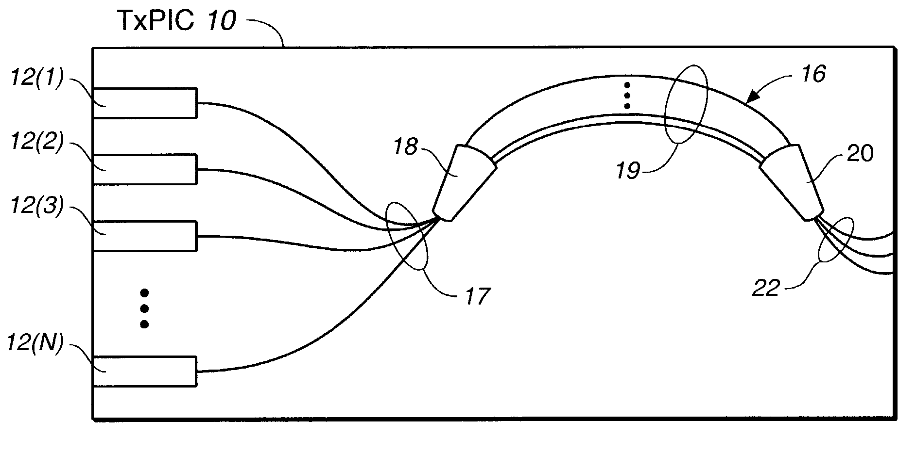
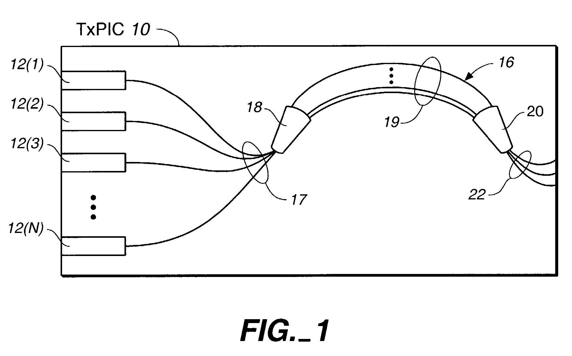
[0061]Reference is now made to FIG. 1 which discloses an InP-based semiconductor TxPIC 10 chip comprising, in monolithic form, a plurality of directly modulated DFB lasers 12(1) . . . 12(N) with their outputs 17 optically coupled to input slab 18 of to an optical combiner, shown here in the form of an arrayed waveguide grating (AWG) 16. AWG 16 comprises input slab or free space region 18 and output slab or free space region 20 between which are a plurality of waveguide gratings 19, all of which is known in the art. The output of AWG 16 is preferably a vernier output where more than one output 22 is provided from the center region of the first order Brillouin zone output of AWG 16. The vernier output 22, as indicated, is greater than one output, preferably equal to or greater than three different outputs, from output slab 20 of AWG 16 so that one of the outputs can be selected having an optimum AWG wavelength grid of aligned grid wavelengths. Thus, through the selection of the best v...


PUM


Abstract

A monolithic photonic integrated circuit (PIC) chip comprises an array of modulated sources providing a plurality of channel signals of different wavelengths and an optical combiner coupled to receive the channel signals and produce a combined output of the channel signals. The arrays of modulated sources are formed as ridge waveguides to enhance the output power from the respective modulated sources so that the average output power from the sources is approximately 2 to 4 times higher than in the case of comparable arrays of modulated sources formed as buried waveguides.

Description

CROSS-REFERENCE TO RELATED APPLICATIONS[0001]This nonprovisional application claims the benefit of priority of provisional applications, Ser. No. 60 / 378,010, filed May 10, 2002 and entitled, TRANSMITTER PHOTONIC INTEGRATED CIRCUIT (TXPIC) CHIP WITH ENHANCED POWER AND YIELD WITHOUT ON-CHIP AMPLIFICATION; Ser. No. 60 / 328,207, filed Oct. 9, 2001 and entitled, PHOTONIC INTEGRATED CIRCUITS FOR DWDM OPTICAL NETWORKS, now U.S. nonprovisional patent application Ser. No. 10 / 267,331, filed Oct. 8, 2002 and entitled. TRANSMITTER PHOTONIC INTEGRATED CIRCUITS (TxPIC) AND OPTICAL TRANSPORT NETWORKS EMPLOYING TxPICs; Ser. No. 60 / 370,345, filed Apr. 5, 2002 and entitled, WAVELENGTH STABILIZATION IN TRANSMITTER PHOTONIC INTEGRATED CIRCUITS (TxPICs), now U.S. nonprovisional patent application, Ser. No. 10 / 267,330, filed Oct. 8, 2002 and entitled, TRANSMITTER PHOTONIC INTEGRATED CIRCUIT (TxPIC) CHIP ARCHITECTURES AND DRIVE SYSTEMS AND WAVELENGTH STABILIZATION FOR TxPICs; Ser. No. 60 / 392,494 filed Jun....

Claims


Application Information

Patent Timeline
IPC IPC(8): G02B6/12H01S5/026H01S5/0625H01S5/12H01S5/20H01S5/22H01S5/40
CPCG02B6/12019H01S5/06258H01S5/4031H01S5/22G02B6/12033H01S5/026H01S5/0265H01S5/12H01S5/204H01S5/205H01S5/106
Inventor JOYNER, CHARLES H.KISH, JR., FRED A.PETERS, FRANK H.MATHUR, ATULWELCH, DAVID F.DENTAI, ANDREW G.LAMBERT, DAMIENSCHNEIDER, RICHARD P.MISSEY, MARK J.
Owner INFINERA CORP
Why Eureka
Try Eureka